GaN on Si EPI wafers Market Size & Forecasts 2026-2035, By Segments (Procurement model, Structure, Application, Industry Vertical), Growth Opportunities, Innovation Landscape, Regulatory Shifts, Strategic Regional Insights (U.S., Japan, China, South Korea, UK, Germany, France), and Competitive Dynamics (IQE, Sumitomo Electric, DOWA Electronics Materials, Mitsubishi Chemical, SK Siltron)
Market Size and Growth Outlook
GaN on Si EPI wafers Market size is anticipated to rise from USD 1.96 billion in 2025 to USD 9.1 billion by 2035, reflecting a CAGR surpassing 16.6% over the forecast horizon of 2026-2035. The estimated revenue for 2026 is USD 2.25 billion.
Get more details on this report
Request Free Sample ReportGaN on Si EPI wafers Market Intelligence Snapshot
Regional Market Dynamics
Segment Momentum
Market Expansion Drivers
Leading Market Participants
Global Market Forecast Snapshot
Market Outlook
Regional and Segment Outlook
Market Growth Drivers and Industry Trends
The rising manufacture of gallium nitride (GaN)-based power and radio frequency (RF) devices directly advances the gan on si EPI wafers market by driving demand for substrates that underpin high-performance semiconductors. Industry leaders like Infineon Technologies and Cree, Inc. have reported ramped production lines, underscoring a shift toward GaN’s superior efficiency and thermal stability compared to traditional silicon. This trend answers growing consumer and industrial preferences for faster, more energy-efficient power conversion and compact RF solutions. For established players, integrating gan on si EPI wafers into scalable, cost-effective production presents an avenue for strengthening supply chain control. New entrants can capitalize on technological niche innovations and partnerships with device makers. Sustained ramp-up in GaN device output prefigures deeper market penetration and the normalization of gan on si EPI wafers as the substrate standard in power and RF applications.
Medium-Term Expansion of EV Fast-Charging and 5G Infrastructure
Accelerated deployment of electric vehicle (EV) fast-charging networks and 5G telecommunications infrastructure propels the gan on si EPI wafers market by creating escalating needs for components that deliver high-power density and fast switching. Regulatory initiatives like the U.S. Department of Energy’s EV fast-charging program and 5G expansion policies across the EU encourage devices leveraging GaN’s advantages, as reflected in Qualcomm’s collaboration with gan on si wafer suppliers. This wave fosters opportunities for incumbents to optimize wafer quality for high-volume manufacturing and for startups to innovate in wafer processing techniques specific to power modules and 5G-specific RF front-ends. The proliferation of these infrastructures will anchor gan on si EPI wafers as a key element in sustaining the speed and efficiency demands characterizing the coming energy and communication landscape.
Long-Term Transition to GaN Wafers in High-Efficiency Electronics
The gradual replacement of traditional silicon with GaN wafers in high-efficiency electronics marks a foundational evolution influencing the gan on si EPI wafers market. Organizations like the International Energy Agency emphasize energy sustainability, reinforcing the strategic movement toward GaN’s higher power efficiency and reduced energy loss. This transition suggests significant opportunities for wafer manufacturers to pioneer material innovations and supply chain robustness while allowing equipment vendors to tailor fabrication technologies accordingly. Corporations such as Texas Instruments publicly highlight investments in GaN-enabled circuits, signaling validation for the substrate’s expanding role. Over time, gan on si EPI wafers are poised to become integral in energy-conscious electronics, positioning market participants to capitalize on a structural shift towards greener, more efficient semiconductor platforms.
Industry Restraints:
High Production Costs and Complex Epitaxial Processes
The intrinsic complexity and expense associated with fabricating GaN on Si EPI wafers present a significant barrier, slowing broader adoption and scale-up. The epitaxial growth of GaN on silicon substrates requires precise control of lattice mismatch and thermal expansion differences, contributing to low yield rates and high manufacturing costs. For instance, Cree, Inc. has highlighted in their technical disclosures that managing defect densities during deposition remains a cost-intensive challenge. These high capital and operational expenditures inhibit smaller firms from entering the market and compel established players to prioritize incremental process optimization over aggressive capacity expansion. Consequently, cost pressures necessitate strategic collaborations and technology-sharing agreements as survival mechanisms. As advanced deposition techniques gradually mature, cost reduction will likely remain incremental, restricting rapid market expansion in the near term while favoring companies with deep process expertise and substantial R&D investments.
Intellectual Property and Technology Licensing Constraints
The GaN on Si EPI wafer arena is encumbered by a complex web of patents and technology licensing agreements, which restrict innovation diffusion and elevate entry barriers. Key players like Sumitomo Electric Industries and Siltronic have secured extensive patent portfolios covering epitaxial growth methods and wafer fabrication, creating a restrictive IP landscape that complicates access for new entrants and smaller innovators. This results in prolonged negotiation cycles and elevated royalty costs, hindering swift product development and commercialization. Established companies gain leverage through exclusive or cross-licensing arrangements, intensifying competition and consolidating market power. Moving forward, intellectual property disputes and licensing negotiations are expected to remain a critical strategic battleground, shaping competitive dynamics and potentially slowing the pace of technological advancement within the GaN on Si EPI wafer segment.
| Growth Driver | Impact on CAGR | Regulatory Influence | Geographic Relevance | Adoption Rate | Impact Timeline |
|---|---|---|---|---|---|
| Increasing production of GaN-based power and RF devices | 1.80% | Short term (≤ 2 yrs) | Asia Pacific (Primary), North America (Spillover) | Medium | Fast |
| Medium-term expansion of EV fast-charging and 5G infrastructure | 1.50% | Medium term (2–5 yrs) | North America (Primary), Europe (Spillover) | High | Moderate |
| Long-term transition to GaN wafers in high-efficiency electronics | 1.20% | Long term (5+ yrs) | Europe (Primary), Asia Pacific (Spillover) | Medium | Moderate |
Unlock insights tailored to your business with our bespoke market research solutions.
Click to get your customized report now.
Regional Demand Dynamics
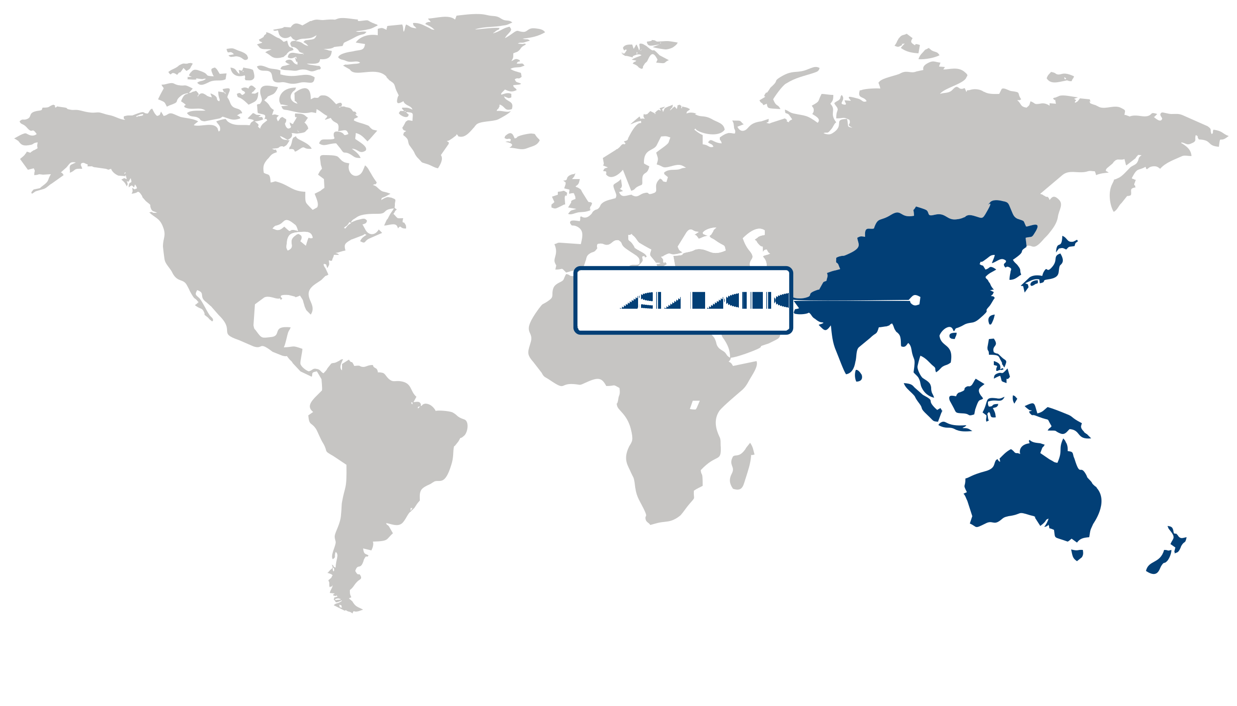
The Asia Pacific gan on si EPI wafers market dominated with approximately 48% share of the global market in 2025, also leading as the fastest-growing region at a 23.24% CAGR. The region’s prominence stems from the dominance of major semiconductor manufacturers such as Samsung and TSMC, coupled with massive investments in 5G infrastructure that are driving robust demand for advanced wafer technology. Government initiatives in South Korea and China supporting semiconductor self-sufficiency further fortify this position, as reported by the Korea Institute of Industrial Technology. These dynamics foster advanced production capabilities and supply chain resilience, enabling players to meet escalating demand for high-performance EPI wafers. Looking ahead, continuous digital transformation and expanding 5G applications establish Asia Pacific as a crucial growth hub, presenting significant opportunities for investors and strategists focused on the gan on si EPI wafers market.
Japan is positioned as a pivotal hub in the Asia Pacific gan on si EPI wafers market, leveraging its advanced semiconductor technology base and strong R&D ecosystem. Japanese companies like Sumitomo Electric and Shin-Etsu Chemical are pivotal in producing high-quality EPI wafers for 5G and power electronics sectors, as noted in their 2024 corporate releases. Japan’s regulatory environment promotes innovation and quality standards, reinforcing its leadership in wafer production. This strategic focus supports the broader regional momentum by supplying cutting-edge materials essential for next-generation semiconductor devices, underpinning Asia Pacific’s dominance.
China anchors the Asia Pacific gan on si EPI wafers market growth through aggressive expansion in semiconductor manufacturing capacity and government-backed initiatives under the “Made in China 2025” strategy. Leading firms such as SMIC and Huawei’s semiconductor arm are rapidly adopting advanced EPI wafer technologies to support the burgeoning 5G ecosystem, as detailed in Ministry of Industry and Information Technology announcements. The rising domestic demand for high-performance chips drives investments in local production, reducing dependency on foreign imports. China’s scale and ambition critically reinforce Asia Pacific’s market leadership while offering immense strategic opportunities within the gan on si EPI wafers market’s value chain.
North America Market Analysis:
North America held a substantial share in the gan on si EPI wafers market, leveraging its advanced semiconductor ecosystem and strong demand for high-performance electronic devices. Key drivers include the region’s focus on innovation in semiconductor fabrication and growing investment in next-generation electronic components, supported by government initiatives such as the U.S. CHIPS Act, which incentivizes domestic chip manufacturing. Leading semiconductor companies headquartered in North America, like Texas Instruments and Cree, increasingly adopt advanced epitaxial wafer technologies to enhance device efficiency and scalability. Additionally, evolving end-user industries such as telecommunications and electric vehicles contribute to steady demand growth. The region’s robust logistics infrastructure and skilled workforce help streamline production and supply chain processes. North America's positioning as a technology front-runner ensures continued opportunities for innovation and expansion in the gan on si EPI wafers market, reinforcing its pivotal role in the global semiconductor landscape.
The United States plays a critical role in North America’s gan on si EPI wafers market, driven by significant R&D investments and supportive policy frameworks. U.S. manufacturers benefit from an ecosystem of specialized suppliers and research institutions like the National Institute of Standards and Technology (NIST), which propels material science advancements essential for epi wafer production. Consumer preference for energy-efficient and high-frequency devices fuels demand in sectors such as 5G infrastructure and renewable energy electronics. Regulatory emphasis on domestic chip manufacturing through legislation like the CHIPS and Science Act stimulates capital inflows, fostering capacity expansions and fresh innovations in gan on si epitaxial wafers. This strategic environment makes the U.S. a key hub for technological breakthroughs, reinforcing its influence across North America and contributing to strong regional market dynamics in the gan on si EPI wafers market.
Europe Market Trends:
Europe maintained notable presence in the gan on si EPI wafers market, driven by its advanced semiconductor ecosystem and strong emphasis on sustainable manufacturing practices. The region’s strategic investments in digital transformation and innovation hubs have accelerated demand for high-performance electronic materials. Regulatory frameworks from entities like the European Union have encouraged environmentally responsible sourcing and production, enhancing market appeal. Supply chain resilience efforts, especially post-pandemic, have further reinforced Europe’s position by minimizing disruptions in semiconductor material availability. Companies such as Infineon Technologies and STMicroelectronics have highlighted their commitment to next-generation wafer technologies, signaling robust industrial adoption. These dynamics, paired with skilled workforce availability and collaborative industry initiatives, position Europe as a pivotal market for gan on si EPI wafers, promising sustained growth opportunities rooted in technological sophistication and regulatory foresight.
Germany played a critical role in the gan on si EPI wafers market, underpinned by its strong manufacturing base and leadership in semiconductor innovation. The country’s focus on integrating Industry 4.0 principles has propelled demand for efficient, high-quality wafer materials tailored to automotive and industrial electronics sectors. German automakers and electronics firms are increasingly adopting gallium nitride technologies for power efficiency, as demonstrated by Bosch’s publicized pilot projects integrating GaN devices. Moreover, government-backed programs like the German Federal Ministry for Economic Affairs and Climate Action’s semiconductor strategy have geared investments toward domestic wafer production capabilities, reducing import dependencies. This strategic emphasis on innovation and supply chain autonomy strengthens Germany’s contribution to Europe’s competitive gan on si EPI wafers market landscape.
France commands a growing position in the gan on si EPI wafers market, fueled by an expanding semiconductor research infrastructure and supportive industrial policies. French entities such as Soitec have advanced epitaxial wafer technologies, fostering innovation that aligns with evolving consumer electronics and telecommunications demands. France’s commitment to green technologies is evident through initiatives coordinated by France’s Ministry of the Economy and Finance, promoting energy-efficient semiconductor components. The robust collaboration between academia, industry, and government, exemplified by public-private partnerships in the French Tech ecosystem, accelerates commercialization of GaN-based applications. France’s progressive regulatory environment and investment in smart manufacturing enhance its role in bolstering Europe’s overall gan on si EPI wafers market competitiveness and resilience.
| Parameter | North America | Asia Pacific | Europe | Latin America | MEA |
|---|---|---|---|---|---|
| Innovation Hub i Scale Nascent Developing Advanced | |||||
| Cost-Sensitive Region i Scale Low Medium High | |||||
| Regulatory Environment i Scale Restrictive Neutral Supportive | |||||
| Demand Drivers i Scale Weak Moderate Strong | |||||
| Development Stage i Scale Emerging Developing Developed | |||||
| Adoption Rate i Scale Low Medium High | |||||
| New Entrants / Startups i Scale Sparse Moderate Dense | |||||
| Macro Indicators i Scale Weak Stable Strong |
Segment Leadership and Growth Trends
GaN on Si EPI wafers Market Share (%), by Procurement model, 2026
Go beyond the chart, access full insights & data tables
Request Free Sample ReportThe gan on si EPI wafers market in 2025 is led by the direct purchase segment, which holds the largest share due to the prevalence of long-term supply agreements between manufacturers and device producers. This stable procurement approach aligns with industry demands for predictable supply chains and cost optimization, fostering deeper partnerships and reliability in production schedules. For instance, Infineon Technologies has emphasized strategic vendor relationships as part of its supply continuity plans. Direct purchase facilitates streamlined inventory management and reduces procurement lead times, offering a competitive edge to established firms while lowering entry barriers for new players through secured sourcing. With increasing integration of GaN devices in automotive and telecom sectors, this segment is expected to maintain its dominance, supported by ongoing efforts to secure resilient and efficient supply frameworks in the near to medium term.
Analysis by Structure
Lateral GaN on Si dominated the gan on si EPI wafers market in 2025, driven primarily by its widespread application in RF and power electronics, essential for 5G infrastructure and next-generation power systems. This structure benefits from mature manufacturing techniques and robust performance characteristics that resonate well with customer preferences for energy efficiency and device miniaturization. The adoption of lateral GaN technology is bolstered by announcements from entities like Qorvo, which highlight advancements in lateral GaN for mobile and defense communications. This segment offers strategic advantages through scalable production and compatibility with existing silicon fabrication lines, thereby attracting both incumbents and startups. Its sustained relevance is rooted in continual innovation meeting the escalating demands of high-frequency, high-efficiency electronics.
Analysis by Application
High power applications represented the largest segment in the gan on si EPI wafers market in 2025, driven by surging demand for efficient power devices and fast-charging systems across consumer electronics and electric vehicle sectors. This surge reflects a consumer shift toward sustainability and energy-saving technologies, reinforced by regulatory pushes such as the U.S. Department of Energy’s initiatives on power efficiency. Leading companies like Navitas Semiconductor emphasize GaN’s superior performance in high power contexts, highlighting robust adoption in EV chargers and industrial power supplies. The segment’s strategic appeal lies in enabling advanced, compact, and highly efficient power solutions, providing fertile ground for innovation and market penetration. Given ongoing digital transformation and electrification trends, high power applications will remain integral to the market’s growth trajectory.
| Segment | Sub-Segment | Largest Segment | Fastest Growing |
|---|---|---|---|
| Procurement model | Tender based, direct purchase | ||
| Structure | Lateral GaN on Si, Vertical GaN on Si, Hybrid GaN on Si | ||
| Application | Low power applications, medium power applications, High power applications, Very high power applications | ||
| Industry Vertical | IT & Telecom, Consumer electronics, Automotive, Aerospace & Defense, Others |
Competitive Landscape and Market Positioning
The competitive environment is marked by significant efforts to enhance technological differentiation and broaden application footprints. Leading players actively deepen alliances with device manufacturers and industrial partners to embed their materials into next-generation systems. Concurrently, investments in refining epitaxial layer uniformity and throughput improvements underscore the race toward cost-effective scalability. Collaborative ventures and technology transfers further consolidate market reach while propelling innovation cycles. Firms such as Mitsubishi Chemical and On Semiconductor leverage their diverse portfolios to cross-fertilize capabilities, expanding their competitive moats. This dynamic fosters a landscape where technological leadership and supply chain resilience become key determinants of market positioning.
Strategic / Actionable Recommendations for Regional Players
North America’s players should emphasize forging synergistic collaborations with semiconductor device developers focusing on power electronics and 5G infrastructure, harnessing emerging epitaxial growth techniques to meet specialized wafer specifications. Strengthening integration with end-use ecosystems will improve market penetration.
In Asia Pacific, companies can capitalize on the expanding semiconductor manufacturing base by aligning with foundries pursuing advanced wafer architectures. Joint innovation efforts and knowledge exchange can accelerate adaptation to localized demand patterns and reinforce supply chain robustness amidst global uncertainties.
European participants may benefit from investing in precision epitaxial technology and sustainability-driven production processes. Partnerships with research institutions and clean energy sectors could unlock value in niche high-performance applications, enhancing differentiation in a competitive geopolitical environment.
| Company | Market Share | Company Revenue | Revenue CAGR (%) | Product Portfolio | Geographic Presence | Innovation / R&D Focus | Strategic Developments |
|---|---|---|---|---|---|---|---|
| No companies available. | |||||||
Industry Development/News
| Company Name | Date | Key Development |
|---|
Customize Your Report
Explore examples of how this report can be tailored to different research needs, including custom segments, additional topics or chapters, and related reports. Click a section of the wheel or its numbered marker to explore the available options.
GaN on Si EPI wafers Market — Custom Segments
| Segment | Sub-Segment |
|---|---|
| No segment data available. | |
GaN on Si EPI wafers Market — Custom TOC
| Custom Chapter | Custom Details | ||
|---|---|---|---|
| No custom TOC data available. | |||
Need a different cut of the data?
Request Custom ResearchWhat is the anticipated CAGR of the GaN on si EPI wafers industry?
Which geographic area exhibits the highest level of GaN on si EPI wafers market penetration?
Which geographical area is witnessing the highest growth rate in the GaN on si EPI wafers sector?
When did direct purchase sub-segment emerge as the largest sub-segment in the procurement model segment of GaN on si EPI wafers sector?
Why is the lateral GaN on si segment leading in the GaN on si EPI wafers industry?
Why does high power applications sub-segment dominate the application segment of GaN on si EPI wafers sector?
How much is the consumer electronics segment expected to grow in the GaN on si EPI wafers industry beyond 2025?
Who are the major participants shaping the GaN on si EPI wafers landscape?
Our Clients
"Working with FBI has been a good experience. The market report provided a holistic view, covering everything from emerging trends to potential risks."
Semtech Corporation
"The experience was highly positive. The team showcased remarkable flexibility in adapting to our specific needs and delivered report that perfectly aligned with all our requirements."
TSMC
"What really stood out to me was how clearly and promptly the Fundamental Business Insights team communicated throughout. It made the collaboration feel effortless."
NXP Semiconductors
Our Research Team & Methodology
Every Fundamental Business Insights report is built by a dedicated vertical research team, validated through a structured primary-and-secondary methodology, and reviewed for accuracy before it reaches you.
Research Team Overview
Prepared by the Electronics & Semiconductors Research Team
Delivery
Published
Demand
Available
Support
Trust & Compliance
Research Domains
10 coverage areasResearch Intelligence
| Source | Reference |
|---|---|
| Semiconductor Industry Association (SIA) | www.semiconductors.org |
| SEMI | www.semi.org |
| JEDEC Solid State Technology Association | www.jedec.org |
| IEEE | www.ieee.org |
| IPC – Association Connecting Electronics Industries | www.ipc.org |
| International Electrotechnical Commission (IEC) | www.iec.ch |
| International Organization for Standardization (ISO) | www.iso.org |
| U.S. Bureau of Industry and Security (BIS) | www.bis.gov |
| U.S. Patent and Trademark Office (USPTO) | www.uspto.gov |
| European Patent Office (EPO) | www.epo.org |
| Taiwan Semiconductor Industry Association (TSIA) | www.tsia.org.tw |
| World Semiconductor Trade Statistics (WSTS) | www.wsts.org |
| International Energy Agency (IEA) | www.iea.org |
| GSMA | www.gsma.com |
| 3GPP | www.3gpp.org |
| ITU (International Telecommunication Union) | www.itu.int |
| Omdia (public insights) | omdia.tech.informa.com |
| Display Supply Chain Consultants (DSCC) | www.displaysupplychain.com |
| U.S. Department of Energy (DOE) | www.energy.gov |
| NIST (National Institute of Standards and Technology) | www.nist.gov |
Research Workflow & Quality Assurance
Data Collection
Verified information gathered through primary and secondary research.
Data Triangulation
Cross-validation using multiple independent data sources.
Forecast Modelling
Market estimates developed using historical trends and analytical models.
Analyst Validation
Findings reviewed by domain experts for accuracy and consistency.
Editorial & Quality Review
Final editorial, quality, and compliance checks before publication.
Final Publication
Released after successful completion of the internal review process.
Report Coverage
📊 Market Assessment
- Market Size & Forecast
- Market Segmentation
- Regional Analysis
- Growth Drivers & Challenges
- Market Dynamics
🏢 Competitive Intelligence
- Competitive Landscape
- Company Profiles
- Competitive Benchmarking
- Mergers & Acquisitions
- Market Share Analysis or Key Company Strategies
🔍 Strategic Analysis
- Value Chain Analysis
- Porter's Five Forces
- PESTLE Analysis
- Pricing Trends
- Supply-Demand Analysis
🚀 Future Outlook
- Technology Landscape
- Regulatory Landscape
- Investment & Funding Landscape
- Emerging Opportunities
- Future Market Outlook
Have a question about this report or need a custom scope?
Request Customization