


Semiconductor Dry Etch Systems Market Size & Growth Forecast 2027–2036, By Segments (Etching Technique, Application, End-use), Regional Demand Trends (North America, Asia Pacific, Europe), Key Country Insights (U.S., Japan, South Korea, Germany, France, Italy), and Competitive Landscape
Market Size and Growth Outlook
Semiconductor Dry Etch Systems Market size was worth USD 17.61 billion in 2026 and is poised to grow at a 5.61% CAGR between 2027 and 2036, surpassing USD 30.4 billion by 2036. The industry revenue for 2027 is assessed at USD 18.44 billion.
Base Year Value (2026)
USD 17.61 billion
CAGR (2027-2036)
5.61%
Forecast Year Value (2036)
USD 30.4 billion

Historical Data Period
2022-2026

Largest Region
North America

Forecast Period
2027-2036
Semiconductor Dry Etch Systems Market Intelligence Snapshot:
-
Regional Market Dynamics:
- North America leads through advanced semiconductor fabrication, a strong equipment supplier base, and continued investment in precise dry etch technologies for complex chip production.
- Asia Pacific is forecast to grow at a 6.67% CAGR as semiconductor manufacturers expand production capacity, increase tool deployments, and upgrade fabrication processes for higher wafer output.
-
Segment Momentum:
- Logic and Memory led the market with a 55.86% share in 2026, supported by high-volume chip manufacturing that depends on precise, repeatable dry etching across complex fabrication processes.
- Power Devices are the fastest-growing application segment as manufacturers require more accurate and controlled etching to produce increasingly specialized, high-performance semiconductor devices.
-
Market Expansion Drivers:
- Semiconductor miniaturization trends increasing demand for precision nanometer-scale etching technologies.
- Growth of AI, IoT, and 5G applications accelerating advanced semiconductor fabrication investments.
- Rising electric vehicle and renewable energy deployments expanding specialized semiconductor manufacturing requirements.
-
Leading Market Participants:
Leading companies in the semiconductor dry etch systems market include Lam Research Corporation (United States), Applied Materials, Inc. (United States), Tokyo Electron Limited (Japan), Hitachi High-Tech Corporation (Japan), Plasma-Therm LLC (United States), Oxford Instruments plc (United Kingdom), NAURA Technology Group Co., Ltd. (China), SPTS Technologies Ltd. (United Kingdom), ULVAC, Inc. (Japan), SAMCO Inc. (Japan).
Global Market Forecast Snapshot:
-
Market Outlook:
- 2026 Market Size: USD 17.61 billion
- 2027 Estimated Market Size: USD 18.44 billion.
- Projected Market Size: USD 30.4 billion by 2036
- Growth Forecasts: 5.61% CAGR (2027-2036)
-
Regional and Segment Outlook:
- Leading Regional Market: North America
- High-Growth Regional Hub: Asia Pacific
- Core Revenue Segment: Deep Reactive Ion Etching (DRIE) (Etching Technique) | Logic and Memory (Application) | Consumer Electronics (End-use)
- Emerging Opportunity Segment: Deep Reactive Ion Etching (DRIE) (Etching Technique) | Power Devices (Application) | Telecommunications (End-use)
Market Growth Drivers and Industry Trends
Semiconductor miniaturization trends increasing demand for precision nanometer-scale etching technologies
The continued push toward smaller semiconductor features is increasing the importance of highly controlled etching processes capable of producing precise structures at increasingly advanced technology nodes. Semiconductor dry etch systems market growth is closely linked to the need for selective material removal during the fabrication of intricate device architectures, where process uniformity and dimensional control are critical to yield and performance. As chip designs incorporate increasingly complex layers and structures, manufacturers require etching technologies that can achieve high aspect ratios while minimizing damage to sensitive materials. Advanced dry etching processes provide the plasma-based control required for precise pattern transfer across sophisticated semiconductor structures, supporting fabrication requirements associated with increasingly dense integrated circuits.
Growth of AI, IoT, and 5G applications accelerating advanced semiconductor fabrication investments
Growing deployment of artificial intelligence, connected devices, and high-speed communication networks is increasing demand for advanced semiconductor components with greater processing capability, energy efficiency, and connectivity performance. This expansion is strengthening the semiconductor dry etch systems market as chip manufacturers invest in fabrication technologies capable of producing sophisticated logic, memory, communication, and sensing devices. AI workloads require advanced processors and high-performance memory, while IoT and 5G applications depend on increasingly capable connectivity and edge devices, creating diverse requirements across semiconductor production. The resulting emphasis on advanced process technologies increases the need for sophisticated etching equipment that can support complex device geometries and multilayer wafer fabrication.
Rising electric vehicle and renewable energy deployments expanding specialized semiconductor manufacturing requirements
The transition toward electric mobility and greater use of renewable energy systems is expanding applications for power semiconductors and other specialized electronic components used in vehicles, charging infrastructure, inverters, energy storage systems, and power management equipment. Demand from these applications is supporting the semiconductor dry etch systems market as manufacturers develop production capacity for devices requiring specialized structures and material combinations. Electric vehicles rely on semiconductor components for power conversion, battery management, motor control, sensing, and connectivity, while renewable energy installations require power electronics to manage electricity generation and grid integration. Expanding semiconductor requirements across these applications are encouraging fabrication investments and increasing the need for process equipment capable of producing reliable and precisely engineered semiconductor structures.
| Growth Driver Assessment Framework | |||||
| Growth Driver | Impact On CAGR | Regulatory Influence | Geographic Relevance | Adoption Rate | Impact Timeline |
|---|---|---|---|---|---|
| Semiconductor miniaturization trends increasing demand for precision nanometer-scale etching technologies | 1.90% | High | Asia Pacific, North America | High | Near Term |
| Growth of AI, IoT, and 5G applications accelerating advanced semiconductor fabrication investments | 1.80% | Moderate | Asia Pacific, Europe | High | Mid Term |
| Rising electric vehicle and renewable energy deployments expanding specialized semiconductor manufacturing requirements | 1.40% | Moderate | Asia Pacific, Europe | Emerging | Long Term |
Unlock insights tailored to your business with our bespoke market research solutions - Click to get your customized report now!
Regional Demand Dynamics
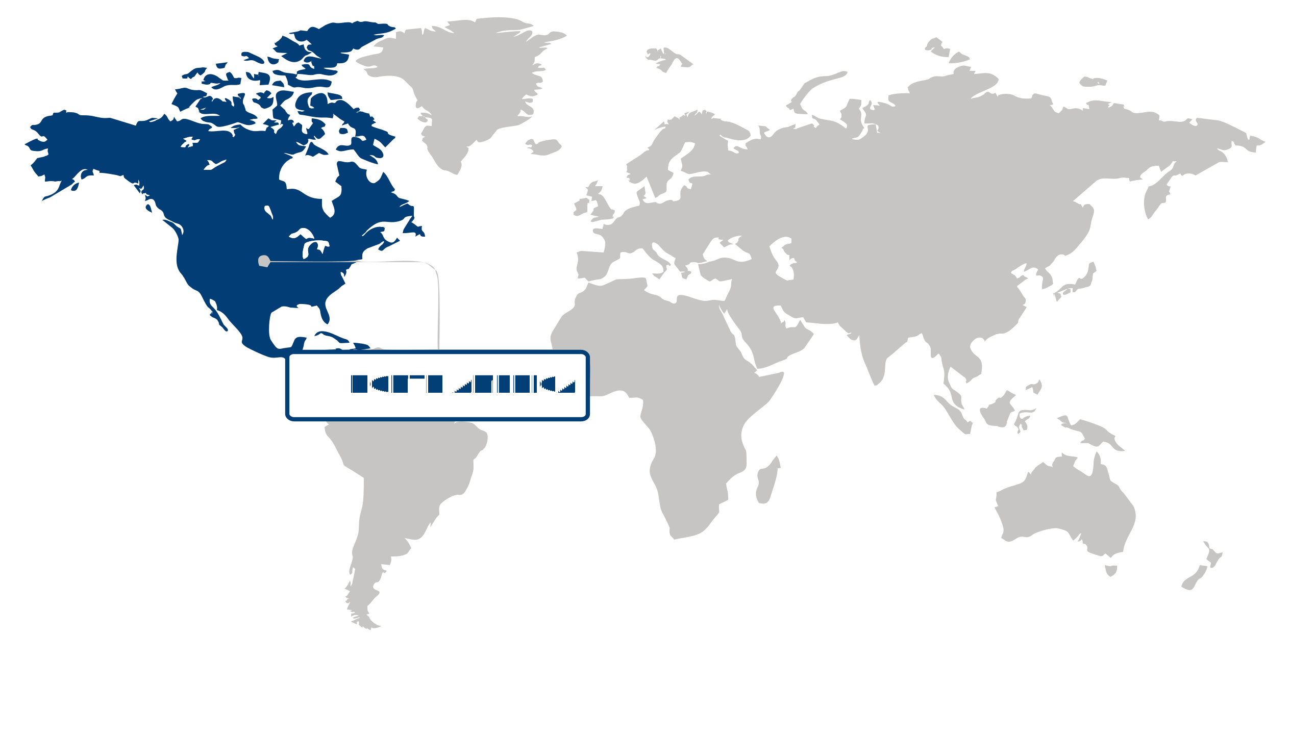
Largest Region
North America
Largest Market Share in 2026
North America (Largest Region) vs Asia Pacific (Fastest-Growing Region)
North America led the semiconductor dry etch systems market in 2026, reflecting its strong semiconductor research ecosystem, advanced fabrication capabilities, and sustained investment in process technologies. The region's established semiconductor infrastructure supports demand for highly precise etching equipment used in the fabrication of increasingly complex devices. Growth in advanced computing, artificial intelligence hardware, high-performance electronics, and other semiconductor applications is encouraging continued investment in fabrication technologies and process control. Strong research capabilities and close integration between semiconductor manufacturing, equipment development, and advanced materials research further reinforce the region's position in the market.
Asia Pacific is the fastest-growing region, supported by its extensive semiconductor manufacturing ecosystem and ongoing expansion of fabrication capacity. Increasing investment in advanced semiconductor facilities is creating demand for sophisticated dry etch systems capable of supporting tighter process requirements and more complex device architectures. The region's concentration of electronics manufacturing also strengthens the connection between semiconductor production and downstream demand for consumer, automotive, communications, and industrial electronics. Government support for domestic semiconductor development, growing fabrication capabilities, and continued technology upgrades are further accelerating adoption of advanced etching equipment.
Key Country Insights
The U.S. semiconductor dry etch systems market is driven by demand for advanced chip fabrication technologies. Equipment suppliers are enhancing process precision, plasma control, and automation capabilities to support increasingly complex semiconductor manufacturing.
Japan continues advancing semiconductor dry etch systems with strong emphasis on precision processing and manufacturing consistency. Equipment manufacturers invest in process optimization and contamination control to meet demanding semiconductor production standards.
South Korea strengthens the semiconductor dry etch systems market through continuous investments in advanced foundry and memory production. Manufacturers seek higher throughput, improved yield, and process flexibility to support next-generation semiconductor devices.
Germany focuses on semiconductor dry etch systems that deliver consistent process performance for advanced manufacturing environments. Companies prioritize engineering excellence, equipment reliability, and integration with sophisticated semiconductor production lines.
France supports semiconductor dry etch systems through research collaborations and specialized semiconductor manufacturing initiatives. The market emphasizes process innovation and advanced equipment capabilities for high-value microelectronics applications.
Italy is expanding semiconductor dry etch system adoption within specialized electronics manufacturing and research facilities. Organizations prioritize equipment modernization and process reliability to strengthen domestic semiconductor production capabilities.
Segment Leadership and Growth Trends
Etching Technique Segment Analysis: Deep Reactive Ion Etching (DRIE) (Largest & Fastest-Growing Segment)
Deep reactive ion etching (DRIE) led the semiconductor dry etch systems market, accounting for a 46.43% share in 2026, while also representing the fastest-growing technique. Its strong position stems from the ability to create deep, high-aspect-ratio structures with precise dimensional control, making it particularly valuable for advanced semiconductor and microfabrication processes. Growing demand for increasingly sophisticated device architectures is reinforcing the need for highly controlled etching, while improvements in process precision, selectivity, and wafer uniformity continue to support DRIE adoption across demanding fabrication applications.
Application Segment Analysis: Logic and Memory (Largest Segment) vs Power Devices (Fastest-Growing Segment)
The logic and memory application segment held the largest share of the semiconductor dry etch systems market at 55.86% in 2026, supported by the extensive use of dry etching throughout advanced semiconductor fabrication. Increasing device complexity and the need for precise pattern transfer across increasingly intricate structures require highly controlled etching processes, sustaining demand from logic and memory manufacturing.
Power devices are emerging as the fastest-growing application, driven by expanding demand for semiconductor components used in electrification, energy management, and power-efficient electronic systems. As manufacturers pursue improved device performance and more sophisticated architectures, dry etch systems are becoming increasingly important for achieving precise feature formation and reliable fabrication outcomes in power semiconductor production.
| Report Segmentation | |||
| Segment | Sub-Segment | Largest Segment | Fastest Growing Segment |
|---|---|---|---|
| Etching Technique | Reactive Ion Etching (RIE), Inductively Coupled Plasma (ICP)Etching, Deep Reactive Ion Etching (DRIE) | Deep Reactive Ion Etching (DRIE) | Deep Reactive Ion Etching (DRIE) |
| Application | Logic and Memory, MEMS and Sensors, Power Devices | Logic and Memory | Power Devices |
| End-use | Consumer Electronics, Automotive, Telecommunications | Consumer Electronics | Telecommunications |
 Read our Research Approach
Competitive Landscape and Market Positioning
Major players in the semiconductor dry etch systems market:
1. Lam Research Corporation (United States)
2. Applied Materials Inc. (United States)
3. Tokyo Electron Limited (Japan)
4. Hitachi High-Tech Corporation (Japan)
5. Plasma-Therm LLC (United States)
6. Oxford Instruments plc (United Kingdom)
7. NAURA Technology Group Co. Ltd. (China)
8. SPTS Technologies Ltd. (United Kingdom)
9. ULVAC Inc. (Japan)
10. SAMCO Inc. (Japan)
Advancements in precision manufacturing are driving continuous innovation in the semiconductor dry etch systems market. Increasing complexity in chip architecture is pushing development toward higher accuracy and process control. Collaborative engineering efforts are supporting faster integration of advanced etching techniques. These developments are reinforcing the transition toward more sophisticated semiconductor fabrication capabilities.
Why Choose Us
Specialized Expertise: Our team comprises industry experts with a deep understanding of your market segment. We bring specialized knowledge and experience that ensures our research and consulting services are tailored to your unique needs.
Customized Solutions: We understand that every client is different. That's why we offer customized research and consulting solutions designed specifically to address your challenges and capitalize on opportunities within your industry.
Proven Results: With a track record of successful projects and satisfied clients, we have demonstrated our ability to deliver tangible results. Our case studies and testimonials speak to our effectiveness in helping clients achieve their goals.
Cutting-Edge Methodologies: We leverage the latest methodologies and technologies to gather insights and drive informed decision-making. Our innovative approach ensures that you stay ahead of the curve and gain a competitive edge in your market.
Client-Centric Approach: Your satisfaction is our top priority. We prioritize open communication, responsiveness, and transparency to ensure that we not only meet but exceed your expectations at every stage of the engagement.
Continuous Innovation: We are committed to continuous improvement and staying at the forefront of our industry. Through ongoing learning, professional development, and investment in new technologies, we ensure that our services are always evolving to meet your evolving needs.
Value for Money: Our competitive pricing and flexible engagement models ensure that you get maximum value for your investment. We are committed to delivering high-quality results that help you achieve a strong return on your investment.
Select Licence Type