


Wafer Vacuum Assembling Equipment Market Size & Growth Forecast 2027–2036, By Segments (Product, Application), Regional Demand Trends (North America, Asia Pacific, Europe), Key Country Insights (U.S., Japan, South Korea, Germany, France, Italy), and Competitive Landscape
Market Size and Growth Outlook
Wafer Vacuum Assembling Equipment Market size stood at USD 2.5 billion in 2026 and is predicted to grow at a 5.23% CAGR from 2027 to 2036, crossing USD 4.16 billion by 2036. The industry revenue for 2027 is calculated at USD 2.61 billion.
Base Year Value (2026)
USD 2.5 billion
CAGR (2027-2036)
5.23%
Forecast Year Value (2036)
USD 4.16 billion

Historical Data Period
2022-2026

Largest Region
Asia Pacific

Forecast Period
2027-2036
Wafer Vacuum Assembling Equipment Market Intelligence Snapshot:
-
Regional Market Dynamics:
- Asia Pacific leads because its extensive semiconductor and electronics manufacturing base generates sustained demand for wafer assembly equipment across high-volume production environments.
- Asia Pacific is projected to grow at a 6.67% CAGR, driven by capacity expansions, process upgrades, and increasing demand for precise, contamination-controlled wafer assembly with improved production yields.
-
Segment Momentum:
- The Semiconductor Industry held a 55.86% share in 2026, driven by its need for precise wafer assembly, contamination control, and consistent processing to maintain production yield and device reliability.
- Electronics Manufacturing is the fastest-growing application segment as producers adopt more precise wafer assembly methods to support increasingly complex devices and tighter manufacturing tolerances.
-
Market Expansion Drivers:
- Rapid semiconductor miniaturization and performance demands increasing precision wafer assembly requirements.
- Expansion of advanced packaging and wide-bandgap semiconductor adoption driving equipment demand.
- Global semiconductor manufacturing capacity expansion strengthening equipment deployment pipelines.
-
Leading Market Participants:
Prominent players in the wafer vacuum assembling equipment market include Applied Materials, Inc. (United States), Tokyo Electron Limited (Japan), Lam Research Corporation (United States), EV Group GmbH (Austria), SUSS MicroTec SE (Germany), Besi Netherlands B.V. (Netherlands), ASMPT Limited (Singapore), Kulicke and Soffa Industries, Inc. (Singapore), Shibaura Mechatronics Corporation (Japan), Tokyo Seimitsu Co., Ltd. (Japan).
Global Market Forecast Snapshot:
-
Market Outlook:
- 2026 Market Size: USD 2.5 billion
- 2027 Estimated Market Size: USD 2.61 billion.
- Projected Market Size: USD 4.16 billion by 2036
- Growth Forecasts: 5.23% CAGR (2027-2036)
-
Regional and Segment Outlook:
- Leading Regional Market: Asia Pacific
- High-Growth Regional Hub: Asia Pacific
- Core Revenue Segment: Fully Automatic Vacuum Assembling Equipment (Product) | Semiconductor Industry (Application)
- Emerging Opportunity Segment: Fully Automatic Vacuum Assembling Equipment (Product) | Electronics Manufacturing (Application)
Market Growth Drivers and Industry Trends
Rapid semiconductor miniaturization and performance demands increasing precision wafer assembly requirements
The continued drive toward smaller semiconductor geometries and higher device performance is making precision increasingly critical in the wafer assembly process, thereby supporting the wafer vacuum assembling equipment market growth. As semiconductor manufacturers work with increasingly compact and complex architectures, assembly equipment must maintain accurate alignment, controlled handling, and contamination-free processing to protect wafer integrity and device reliability. Vacuum-based assembly environments are particularly valuable where sensitive semiconductor materials and components require protection from particles, moisture, and other contaminants, while advanced automation and process-control capabilities help manufacturers maintain consistency during increasingly demanding assembly operations.
Expansion of advanced packaging and wide-bandgap semiconductor adoption driving equipment demand
The growing use of advanced packaging architectures and wide-bandgap semiconductor materials is creating new equipment requirements across semiconductor manufacturing, strengthening demand in the wafer vacuum assembling equipment market. Technologies based on materials such as silicon carbide and gallium nitride require specialized handling and assembly processes because of their distinct material properties and applications in power electronics, electric mobility, renewable energy, and high-performance systems. At the same time, advanced packaging approaches place greater emphasis on precise bonding, alignment, thermal management, and compact integration, encouraging manufacturers to deploy vacuum assembly equipment capable of supporting increasingly sophisticated production processes.
Global semiconductor manufacturing capacity expansion strengthening equipment deployment pipelines
Expansion of semiconductor fabrication and packaging capacity across major manufacturing regions is increasing the need for production equipment throughout the supply chain, including specialized wafer assembly systems. This capacity growth will propel the wafer vacuum assembling equipment market as manufacturers establish new facilities, expand existing production lines, and upgrade equipment to support higher-volume and more advanced semiconductor output. Investment in localized semiconductor production is also encouraging the development of additional assembly and packaging capabilities, creating procurement opportunities for equipment that can provide controlled processing environments, repeatable performance, and compatibility with automated manufacturing workflows.
| Growth Driver Assessment Framework | |||||
| Growth Driver | Impact On CAGR | Regulatory Influence | Geographic Relevance | Adoption Rate | Impact Timeline |
|---|---|---|---|---|---|
| Rapid semiconductor miniaturization and performance demands increasing precision wafer assembly requirements | 2.80% | High | Asia Pacific, North America | High | Near Term |
| Expansion of advanced packaging and wide-bandgap semiconductor adoption driving equipment demand | 2.40% | High | Asia Pacific, Europe | High | Near Term |
| Global semiconductor manufacturing capacity expansion strengthening equipment deployment pipelines | 1.90% | High | Asia Pacific, North America, Europe | Medium | Mid Term |
Unlock insights tailored to your business with our bespoke market research solutions - Click to get your customized report now!
Regional Demand Dynamics
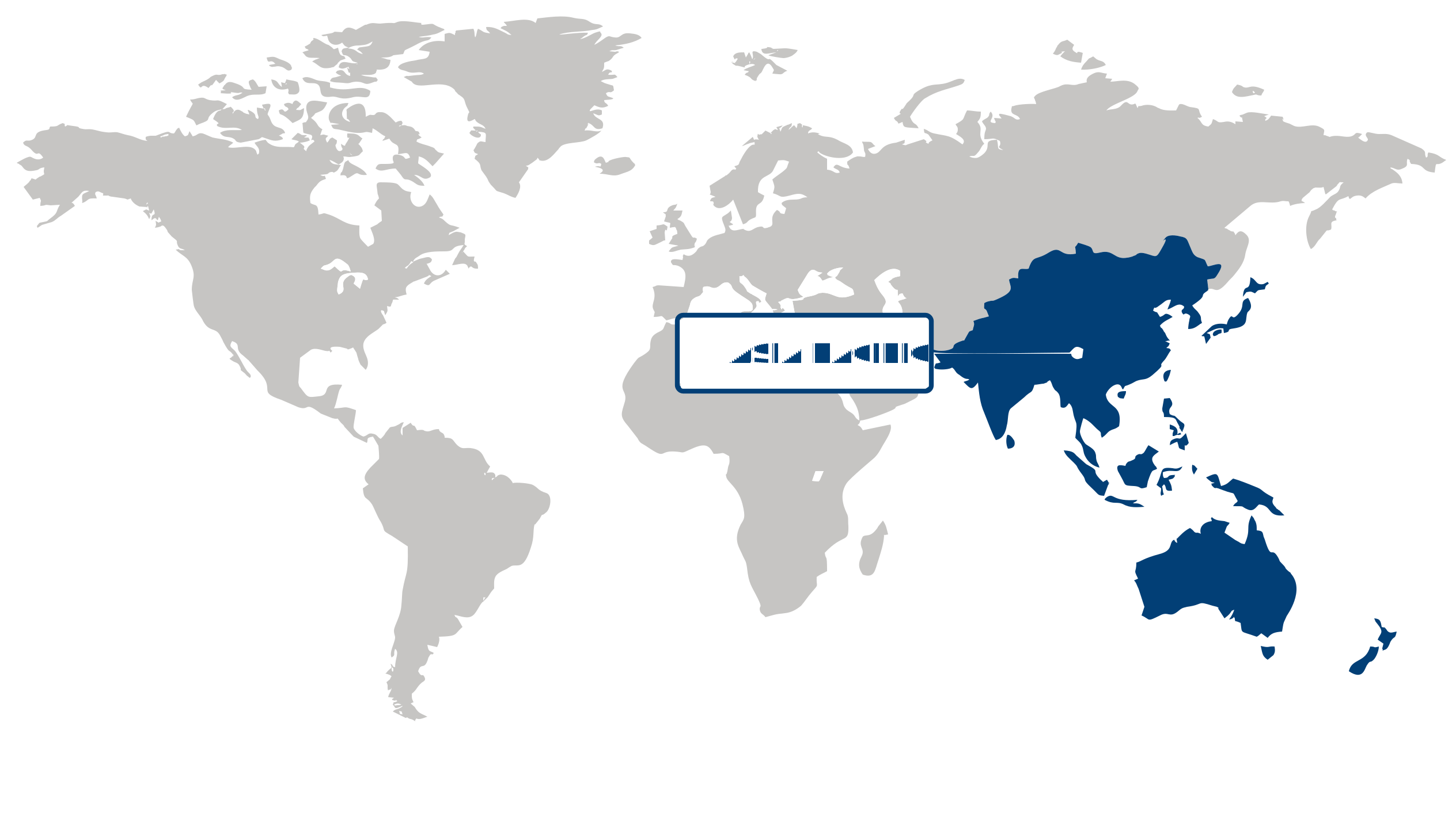
Largest Region
Asia Pacific
Largest Market Share in 2026
Asia Pacific (Largest & Fastest-Growing Region)
Asia Pacific dominated the wafer vacuum assembling equipment market in 2026 and also emerged as the fastest-growing regional market, supported by its extensive semiconductor manufacturing ecosystem and continued expansion of advanced electronics production. The region benefits from strong investment in wafer fabrication capacity, packaging technologies, and automation systems as manufacturers seek greater production precision and process efficiency. Rising demand for semiconductors across consumer electronics, telecommunications, automotive applications, and industrial equipment is increasing the need for sophisticated vacuum-based assembly solutions. In addition, the concentration of component suppliers, manufacturing facilities, and technology-focused industrial infrastructure supports faster equipment deployment and innovation. Ongoing efforts to strengthen domestic semiconductor capabilities and modernize fabrication operations are further reinforcing Asia Pacific's leadership and growth prospects.
Key Country Insights
The U.S. wafer vacuum assembling equipment market benefits from growing investment in semiconductor packaging and advanced device manufacturing. Equipment suppliers are improving alignment precision, automation, and production efficiency for high-performance applications.
Japan prioritizes wafer vacuum assembling equipment capable of supporting complex semiconductor assembly with exceptional accuracy. Equipment developers continue refining automation and contamination control to meet demanding fabrication requirements.
South Korea is investing in wafer vacuum assembling equipment to support expanding semiconductor manufacturing and advanced packaging operations. Companies are enhancing production efficiency and equipment compatibility with high-volume fabrication facilities.
Germany emphasizes wafer vacuum assembling equipment designed for highly accurate semiconductor assembly processes. Manufacturers focus on equipment durability, process stability, and seamless integration with advanced production environments.
France supports wafer vacuum assembling equipment through continued development of domestic microelectronics and semiconductor research capabilities. Organizations prioritize precision assembly technologies that improve production quality and manufacturing consistency.
Italy is strengthening wafer vacuum assembling equipment adoption within specialized semiconductor manufacturing and research applications. Equipment investments emphasize flexible production, process accuracy, and support for advanced electronic component assembly.
Segment Leadership and Growth Trends
Product Segment Analysis: Fully Automatic Vacuum Assembling Equipment (Largest & Fastest-Growing Segment)
Fully automatic vacuum assembling equipment accounted for a 46.43% share of the wafer vacuum assembling equipment market in 2026 and was also the fastest-growing product segment. Its combined position reflects the semiconductor industry's emphasis on high-precision, repeatable assembly processes that minimize manual intervention and maintain consistent manufacturing quality. Automation improves process control, reduces the potential for handling-related inconsistencies, and supports efficient production environments where wafer integrity and assembly precision are critical.
Application Segment Analysis: Semiconductor Industry (Largest Segment) vs Electronics Manufacturing (Fastest-Growing Segment)
In the wafer vacuum assembling equipment market, the semiconductor industry represented the largest application segment with a 55.86% share in 2026. The segment benefits from the stringent cleanliness, precision, and controlled-environment requirements associated with wafer processing and assembly, where vacuum-based equipment helps protect sensitive components while supporting reliable manufacturing workflows.
Electronics manufacturing is advancing as the fastest-growing application as increasingly sophisticated electronic products require precise handling and assembly of miniaturized components. Greater automation, rising quality expectations, and the continued integration of advanced semiconductor components into electronic systems are strengthening demand for vacuum assembly technologies capable of delivering consistent and contamination-controlled processes.
| Report Segmentation | |||
| Segment | Sub-Segment | Largest Segment | Fastest Growing Segment |
|---|---|---|---|
| Product | Manual Vacuum Assembling Equipment, Semi-Automatic Vacuum Assembling Equipment, Fully Automatic Vacuum Assembling Equipment | Fully Automatic Vacuum Assembling Equipment | Fully Automatic Vacuum Assembling Equipment |
| Application | Semiconductor Industry, Solar Panel Manufacturing, Electronics Manufacturing | Semiconductor Industry | Electronics Manufacturing |
 Read our Research Approach
Competitive Landscape and Market Positioning
Leading companies in the wafer vacuum assembling equipment market:
1. Applied Materials Inc. (United States)
2. Tokyo Electron Limited (Japan)
3. Lam Research Corporation (United States)
4. EV Group GmbH (Austria)
5. SUSS MicroTec SE (Germany)
6. Besi Netherlands B.V. (Netherlands)
7. ASMPT Limited (Singapore)
8. Kulicke and Soffa Industries Inc. (Singapore)
9. Shibaura Mechatronics Corporation (Japan)
10. Tokyo Seimitsu Co. Ltd. (Japan)
The wafer vacuum assembling equipment market is evolving with a strong emphasis on precision handling and contamination-free assembly processes. Equipment innovation is increasingly focused on improving stability and throughput efficiency. New system designs are incorporating enhanced control mechanisms to support advanced semiconductor manufacturing requirements. This progression is strengthening performance reliability and process consistency.
Industry Development/News
| Company Name | Date | Key Development |
|---|---|---|
| SA-Foundry sp. z o.o. | Oct-23 | SA-Foundry sp. z o.o. completed a dedicated high-pressure die casting facility for premium aluminum alloy casting production tailored to a specific client. The facility enhances specialized manufacturing capacity and supports expanded output of high-precision metal components used in industrial and semiconductor-related applications. |
| Applied Materials, Inc. | Feb-25 | Applied Materials introduced its Advanced Packaging Solutions platform designed for high-density 3D chip stacking and wafer-level integration. The platform targets AI and high-performance computing applications, improving bonding precision, throughput, and enabling advanced semiconductor packaging scalability. |
| Tokyo Electron Limited | Jan-25 | Tokyo Electron expanded production capacity for advanced packaging equipment at its Miyagi facility in Japan to address rising global demand for wafer bonding and alignment systems. The expansion strengthens supply capabilities for advanced semiconductor assembly and wafer-level integration technologies. |
| KLA Corporation | Dec-24 | KLA Corporation acquired FemtoMetrix, an AI-driven metrology company, to enhance process control and inspection capabilities for advanced semiconductor packaging. The acquisition strengthens wafer-level manufacturing precision and supports next-generation assembly and quality monitoring systems. |
| Lam Research Corporation | Oct-24 | Lam Research introduced enhancements to its Coronus and Syndion product lines, improving plasma processing performance and wafer-level packaging capabilities. The upgrades support advanced node scaling and heterogeneous integration in next-generation semiconductor manufacturing. |
| EV Group (EVG) | Jun-24 | EV Group secured multiple high-volume manufacturing orders for GEMINI wafer bonding systems supporting advanced 3D and heterogeneous integration applications. The orders reinforce adoption of wafer-level bonding technologies across semiconductor manufacturers scaling advanced packaging production. |
Why Choose Us
Specialized Expertise: Our team comprises industry experts with a deep understanding of your market segment. We bring specialized knowledge and experience that ensures our research and consulting services are tailored to your unique needs.
Customized Solutions: We understand that every client is different. That's why we offer customized research and consulting solutions designed specifically to address your challenges and capitalize on opportunities within your industry.
Proven Results: With a track record of successful projects and satisfied clients, we have demonstrated our ability to deliver tangible results. Our case studies and testimonials speak to our effectiveness in helping clients achieve their goals.
Cutting-Edge Methodologies: We leverage the latest methodologies and technologies to gather insights and drive informed decision-making. Our innovative approach ensures that you stay ahead of the curve and gain a competitive edge in your market.
Client-Centric Approach: Your satisfaction is our top priority. We prioritize open communication, responsiveness, and transparency to ensure that we not only meet but exceed your expectations at every stage of the engagement.
Continuous Innovation: We are committed to continuous improvement and staying at the forefront of our industry. Through ongoing learning, professional development, and investment in new technologies, we ensure that our services are always evolving to meet your evolving needs.
Value for Money: Our competitive pricing and flexible engagement models ensure that you get maximum value for your investment. We are committed to delivering high-quality results that help you achieve a strong return on your investment.
Select Licence Type