3D Semiconductor Packaging Market Size & Growth Forecast 2027–2036, By Segments (Material, End-Use Industry, Technology), Regional Demand Trends (North America, Asia Pacific, Europe), Key Country Insights (U.S., Japan, South Korea, Germany, France, Italy), and Competitive Landscape
Market Size and Growth Outlook
3D Semiconductor Packaging Market size was more than USD 14.41 Billion in 2026 and is set to grow at 18.72% CAGR between 2027 and 2036, reaching USD 80.15 Billion by 2036. The industry revenue for 2027 is assessed at USD 16.74 Billion.
Get more details on this report
Request Free Sample Report3D Semiconductor Packaging Market Intelligence Snapshot
Regional Market Dynamics
- North America held a 37.8% share in 2026, supported by semiconductor research, high-performance computing demand, advanced chip investments, and efforts to strengthen domestic manufacturing.
- Asia Pacific is expanding fastest through its electronics manufacturing ecosystem, growing semiconductor capacity, packaging investments, and rising demand for high-density integration.
Segment Momentum
- The automotive segment led the market in 2026, driven by growing use of advanced electronics in driver assistance systems, infotainment platforms, and electric powertrains that require compact and reliable semiconductor packaging.
- 3D Wafer-Level Chip-Scale Packaging (WL-CSP) is projected to grow the fastest as manufacturers seek smaller package sizes, improved electrical performance, and efficient production for mobile and wearable electronics.
Market Expansion Drivers
- Rising demand for high-performance miniaturized semiconductor devices across advanced electronics
- Expanding data centers and cloud computing infrastructure driving advanced packaging demand
- Automotive electrification and ADAS integration accelerating heterogeneous chip packaging adoption
Leading Market Participants
- Top players in the 3D semiconductor packaging market include Taiwan Semiconductor Manufacturing Company Limited (Taiwan), Intel Corporation (United States), Samsung Electronics Co., Ltd. (South Korea), SK Hynix Inc. (South Korea), Micron Technology, Inc. (United States), Advanced Semiconductor Engineering, Inc. (Taiwan), Amkor Technology, Inc. (United States), JCET Group Co., Ltd. (China), STMicroelectronics N.V. (Switzerland), Texas Instruments Incorporated (United States)
Global Market Forecast Snapshot
Market Outlook
- 2026 Market Size: USD 14.41 Billion
- 2027 Estimated Market Size: USD 16.74 Billion
- Projected Market Size: USD 80.15 Billion by 2036
- Growth Forecast: 18.72% CAGR (2027-2036)
Regional and Segment Outlook
- Leading Regional Market: North America
- High-Growth Regional Hub: Asia Pacific
- Core Revenue Segment: Organic Substrates (Material) | Automotive (End-Use Industry) | 3D Through Silicon via (Technology)
- Emerging Opportunity Segment: Organic Substrates (Material) | Healthcare (End-Use Industry) | 3D Wafer-Level Chip-Scale Packaging (WL-CSP) (Technology)
Market Growth Drivers and Industry Trends
Rising demand for high-performance miniaturized semiconductor devices across advanced electronics
Continuous innovation in consumer electronics, high-performance computing, and intelligent connected devices is increasing the need for semiconductor solutions that deliver greater functionality within increasingly compact form factors. This trend will drive the 3D semiconductor packaging market growth as manufacturers adopt advanced packaging technologies that improve device performance, reduce signal latency, and optimize space utilization. Three-dimensional integration enables closer interconnection between semiconductor components, supporting higher processing efficiency, improved power management, and enhanced thermal performance for sophisticated electronic products where conventional packaging approaches face physical and performance limitations.
Expanding data centers and cloud computing infrastructure driving advanced packaging demand
The rapid expansion of cloud services and digital infrastructure is creating strong demand for semiconductor components capable of supporting intensive computing workloads and high-speed data processing. The 3D semiconductor packaging market benefits from this shift because advanced packaging architectures enable higher bandwidth, lower power consumption, and improved integration of processors with memory technologies used in modern data center environments. These capabilities help optimize computing efficiency while supporting increasingly complex artificial intelligence, analytics, and cloud-based applications that require reliable performance under sustained processing demands.
Automotive electrification and ADAS integration accelerating heterogeneous chip packaging adoption
Growing adoption of electric vehicles and advanced driver assistance systems is increasing the complexity of automotive electronics, requiring highly integrated semiconductor solutions capable of supporting multiple computing functions within limited space. This evolution will propel the 3D semiconductor packaging market growth by encouraging heterogeneous integration of processors, sensors, memory, and specialized accelerators into compact, high-performance packages. Advanced packaging techniques also contribute to improved thermal management, signal integrity, and operational reliability, all of which are essential for automotive environments where electronic systems must perform consistently under demanding operating conditions.
| Growth Driver | Impact on CAGR | Regulatory Influence | Geographic Relevance | Adoption Rate | Impact Timeline |
|---|---|---|---|---|---|
| Rising demand for high-performance miniaturized semiconductor devices across advanced electronics | 2% | High | Asia Pacific, North America | High | Near Term |
| Expanding data centers and cloud computing infrastructure driving advanced packaging demand | 1.9% | High | North America, Asia Pacific | High | Near Term |
| Automotive electrification and ADAS integration accelerating heterogeneous chip packaging adoption | 1.8% | High | Europe, Asia Pacific | High | Near Term |
Unlock insights tailored to your business with our bespoke market research solutions.
Click to get your customized report now.
Regional Demand Dynamics
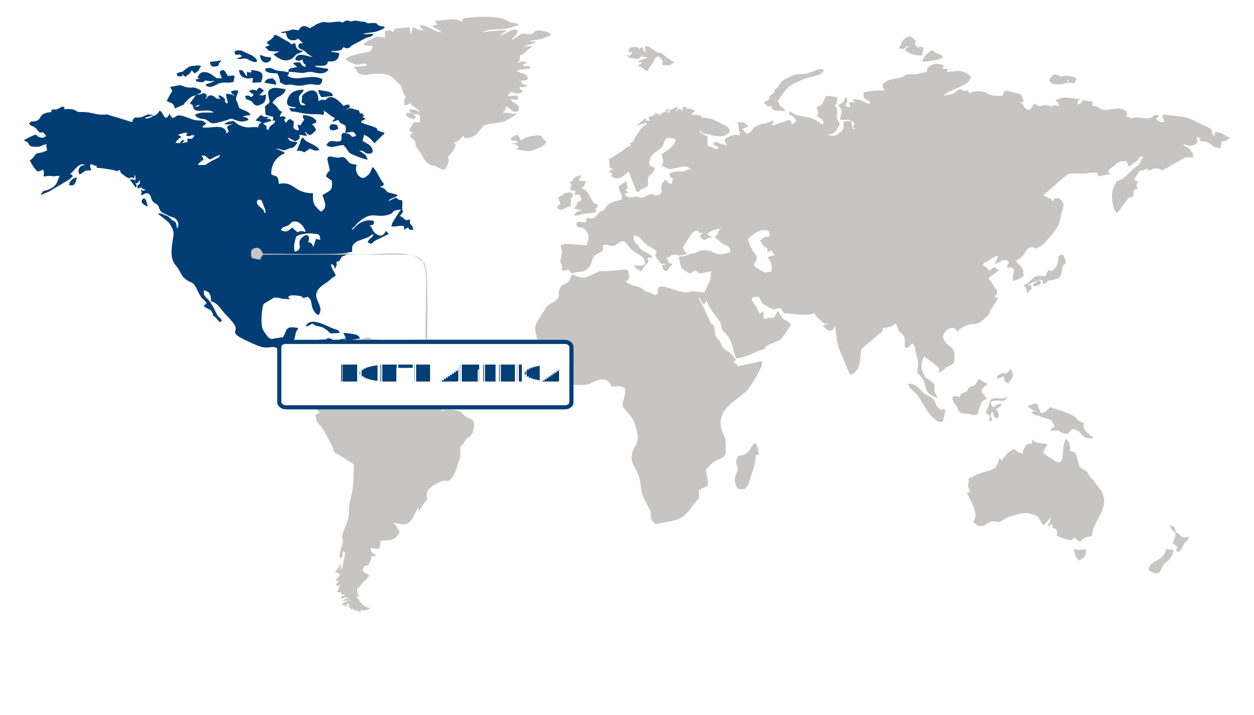
North America (Largest Region)
North America accounted for 37.8% of the 3D semiconductor packaging market in 2026, supported by strong semiconductor research capabilities, demand for high-performance computing, and continued investment in advanced chip technologies. The growing complexity of electronic systems is increasing the need for packaging approaches that improve performance, integration, and space efficiency. Expansion of artificial intelligence, data centers, telecommunications, and high-performance computing is further creating demand for advanced semiconductor packaging solutions. In addition, efforts to strengthen domestic semiconductor manufacturing and develop resilient technology supply chains are supporting investments in sophisticated packaging infrastructure and capabilities across the region.
Asia Pacific (Fastest-Growing Region)
Asia Pacific is expected to register the fastest growth in the 3D semiconductor packaging market, driven by its extensive electronics manufacturing ecosystem, expanding semiconductor production capacity, and increasing demand for compact, high-performance devices. The region's strong presence in consumer electronics, telecommunications, automotive electronics, and industrial technology provides a broad application base for advanced packaging. Rising investments in semiconductor fabrication, packaging, and testing infrastructure are further improving regional capabilities. The increasing adoption of artificial intelligence, edge computing, and connected technologies is also encouraging demand for higher-density semiconductor integration, strengthening opportunities for 3D packaging solutions.
| Parameter | North America | Asia Pacific | Europe | Latin America | MEA |
|---|---|---|---|---|---|
| Innovation Hub i Scale Nascent Developing Advanced | |||||
| Cost-Sensitive Region i Scale Low Medium High | |||||
| Regulatory Environment i Scale Restrictive Neutral Supportive | |||||
| Demand Drivers i Scale Weak Moderate Strong | |||||
| Development Stage i Scale Emerging Developing Developed | |||||
| Adoption Rate i Scale Low Medium High | |||||
| New Entrants / Startups i Scale Sparse Moderate Dense | |||||
| Macro Indicators i Scale Weak Stable Strong |
Key Country Insights
United States 🇺🇸
Advanced Chip IntegrationThe U.S. strengthens investment in 3D semiconductor packaging to support high-performance computing, artificial intelligence, and advanced defense electronics. Companies are expanding packaging capabilities that improve chip performance, integration density, and manufacturing flexibility.
Germany 🇩🇪
Automotive Packaging ExpertiseGermany applies 3D semiconductor packaging to automotive electronics, industrial automation, and high-reliability semiconductor applications. Manufacturers emphasize packaging technologies that enhance thermal management and long-term performance under demanding operating conditions.
Japan 🇯🇵
Precision Packaging DevelopmentJapan continues refining 3D semiconductor packaging through expertise in advanced materials, semiconductor equipment, and precision manufacturing. Domestic suppliers focus on improving package reliability, miniaturization, and production quality for advanced electronic devices.
South Korea 🇰🇷
Memory Packaging AdvancementSouth Korea expands 3D semiconductor packaging capabilities to complement advanced memory and logic semiconductor production. Investment priorities include higher interconnect density, improved manufacturing efficiency, and packaging solutions tailored for artificial intelligence workloads.
France 🇫🇷
Research-Driven PackagingFrance supports 3D semiconductor packaging through collaborative research, specialized electronics manufacturing, and advanced technology development. Companies concentrate on innovative packaging processes that improve performance for industrial, aerospace, and secure electronic applications.
Italy 🇮🇹
Specialized Electronics ManufacturingItaly is strengthening its role in 3D semiconductor packaging through specialized electronics production and partnerships across the semiconductor value chain. Market participants prioritize reliable packaging solutions for industrial, automotive, and precision electronic systems.
Segment Leadership and Growth Trends
3D Semiconductor Packaging Market Share (%), by material, 2026
Go beyond the chart, access full insights & data tables
Request Free Sample ReportMaterial Segment Analysis: Organic Substrates (Largest & Fastest-Growing Segment)
The 3D semiconductor packaging market was led by the organic substrates material segment in 2026, which also emerged as the fastest-growing segment. Organic substrates have become the preferred material because they provide excellent electrical performance, design flexibility, and compatibility with advanced packaging architectures while supporting high-density interconnections. Their ability to accommodate increasingly complex semiconductor designs and deliver cost-effective manufacturing solutions has strengthened their adoption across multiple electronic applications. Ongoing advancements in packaging technologies and the growing demand for high-performance semiconductor devices continue to reinforce the prominence of organic substrates.
End-Use Industry Segment Analysis: Automotive (Largest Segment) vs Healthcare (Fastest-Growing Segment)
The automotive end-use industry segment held the largest share of the 3D semiconductor packaging market in 2026. The increasing integration of advanced electronic systems in modern vehicles, including driver assistance technologies, infotainment platforms, and electric powertrain components, has significantly increased the need for compact, high-performance semiconductor packages. The industry's continued focus on enhanced reliability, thermal management, and miniaturization further supports the widespread adoption of advanced 3D packaging solutions.
The healthcare end-use industry segment is anticipated to witness the fastest growth due to the expanding use of sophisticated medical electronics, wearable health devices, diagnostic equipment, and remote patient monitoring systems. As healthcare technologies become increasingly compact and data-intensive, demand is rising for semiconductor packaging solutions that deliver improved performance, reduced form factors, and enhanced reliability in critical medical applications.
Technology Segment Analysis: 3D Through Silicon via (Largest Segment) vs 3D Wafer-Level Chip-Scale Packaging (WL-CSP) (Fastest-Growing Segment)
The 3D through silicon via technology segment held the largest share of the 3D semiconductor packaging market in 2026. Its dominant position is supported by its capability to provide high-bandwidth communication, shorter interconnect lengths, and superior power efficiency while enabling the vertical integration of multiple semiconductor dies. These advantages make it well suited for high-performance computing, memory devices, and advanced consumer electronics that require greater processing capability within compact footprints.
The 3D wafer-level chip-scale packaging (WL-CSP) technology segment is expected to record the fastest growth as manufacturers increasingly prioritize smaller package sizes, improved electrical performance, and streamlined production processes. The technology supports lightweight and highly integrated semiconductor devices, making it particularly attractive for next-generation mobile electronics, wearable devices, and other applications where space optimization and performance are critical.
| Segment | Sub-Segment | Largest Segment | Fastest Growing |
|---|---|---|---|
| Material | Organic Substrates, Bonding Wires, Lead Frames, Ceramic Packages, Encapsulation Resins, Others | Organic Substrates | Organic Substrates |
| End-Use Industry | Consumer Electronics, Automotive, Healthcare, IT & Telecommunications, Industrial, Aerospace and Defense, Others | Automotive | Healthcare |
| Technology | 3D Through Silicon Via, 3D Package on Package, 3D Wafer-Level Chip-Scale Packaging (WL-CSP), 3D System-on-Chip (3D SoC), 3D Integrated Circuit (3D IC) | 3D Through Silicon via | 3D Wafer-Level Chip-Scale Packaging (WL-CSP) |
Competitive Landscape and Market Positioning
Key companies in the 3D semiconductor packaging market:
- Taiwan Semiconductor Manufacturing Company Limited (Taiwan)
- Intel Corporation (United States)
- Samsung Electronics Co., Ltd. (South Korea)
- SK Hynix, Inc. (South Korea)
- Micron Technology, Inc. (United States)
- Advanced Semiconductor Engineering, Inc. (Taiwan)
- Amkor Technology, Inc. (United States)
- JCET Group Co., Ltd. (China)
- STMicroelectronics N.V. (Switzerland)
- Texas Instruments Incorporated (United States)
As advanced computing, artificial intelligence, and high-performance electronics place greater demands on chip integration, competition in the 3D semiconductor packaging market is increasingly centered on manufacturing sophistication rather than conventional production scale. Participants are investing in advanced stacking technologies, heterogeneous integration capabilities, and process optimization to support higher performance within tighter power and space constraints. At the same time, the ability to coordinate design, packaging, testing, and supply chain activities has become a meaningful differentiator, encouraging closer alignment across the semiconductor value chain as customers seek reliable pathways from prototype development to high-volume commercialization.
| Company | Market Share | Company Revenue | Revenue CAGR (%) | Product Portfolio | Geographic Presence | Innovation / R&D Focus | Strategic Developments |
|---|---|---|---|---|---|---|---|
| Taiwan Semiconductor Manufacturing Company Limited (Taiwan) | |||||||
| Intel Corporation (United States) | |||||||
| Samsung Electronics Co. Ltd. (South Korea) | |||||||
| SK Hynix Inc. (South Korea) | |||||||
| Micron Technology Inc. (United States) | |||||||
| Advanced Semiconductor Engineering Inc. (Taiwan) | |||||||
| Amkor Technology Inc. (United States) | |||||||
| JCET Group Co. Ltd. (China) | |||||||
| STMicroelectronics N.V. (Switzerland) | |||||||
| Texas Instruments Incorporated (United States) |
Industry Development/News
| Company Name | Date | Key Development |
|---|
Customize Your Report
Explore examples of how this report can be tailored to different research needs, including custom segments, additional topics or chapters, and related reports. Click a section of the wheel or its numbered marker to explore the available options.
3D Semiconductor Packaging Market — Custom Segments
| Segment | Sub-Segment |
|---|---|
| Package Function | Memory, Logic and Compute, Mixed-Signal and Analog, RF and Connectivity |
| Manufacturing Process | Wafer-Level Assembly, Die-Level Assembly, Hybrid Bonding, Thermo-Compression Bonding |
| Manufacturing Responsibility | Integrated Device Manufacturer (IDM), Foundry-Led, Outsourced Semiconductor Assembly and Test (OSAT) |
3D Semiconductor Packaging Market — Custom TOC
| Custom Chapter | Custom Details |
|---|---|
| Chiplet Ecosystem & Integration Strategies |
|
| Thermal Management & Power Delivery Priorities |
|
| AI & High-Performance Computing Packaging Roadmaps |
|
Need a different cut of the data?
Request Custom ResearchHow much revenue does the 3D semiconductor packaging market generate?
How is the 3D semiconductor packaging industry size expected to evolve during the forecast period?
How is data center expansion shaping demand for 3D semiconductor packaging?
How are automotive electrification and ADAS influencing packaging strategies?
Which end-use industry leads the 3D semiconductor packaging market?
Which technology segment is expected to grow the fastest in the 3D semiconductor packaging market?
Why does North America lead the 3D semiconductor packaging market?
How is Asia Pacific driving faster growth in 3D semiconductor packaging?
What are the prominent companies operating in the 3D semiconductor packaging landscape?
Our Clients
"Working with FBI has been a good experience. The market report provided a holistic view, covering everything from emerging trends to potential risks."
Semtech Corporation
"The experience was highly positive. The team showcased remarkable flexibility in adapting to our specific needs and delivered report that perfectly aligned with all our requirements."
TSMC
"What really stood out to me was how clearly and promptly the Fundamental Business Insights team communicated throughout. It made the collaboration feel effortless."
NXP Semiconductors
Our Research Team & Methodology
Every Fundamental Business Insights report is built by a dedicated vertical research team, validated through a structured primary-and-secondary methodology, and reviewed for accuracy before it reaches you.
Research Team Overview
Prepared by the Electronics & Semiconductors Research Team
Delivery
Published
Demand
Available
Support
Trust & Compliance
Research Domains
10 coverage areasResearch Intelligence
| Source | Reference |
|---|---|
| Semiconductor Industry Association (SIA) | www.semiconductors.org |
| SEMI | www.semi.org |
| JEDEC Solid State Technology Association | www.jedec.org |
| IEEE | www.ieee.org |
| IPC – Association Connecting Electronics Industries | www.ipc.org |
| International Electrotechnical Commission (IEC) | www.iec.ch |
| International Organization for Standardization (ISO) | www.iso.org |
| U.S. Bureau of Industry and Security (BIS) | www.bis.gov |
| U.S. Patent and Trademark Office (USPTO) | www.uspto.gov |
| European Patent Office (EPO) | www.epo.org |
| Taiwan Semiconductor Industry Association (TSIA) | www.tsia.org.tw |
| World Semiconductor Trade Statistics (WSTS) | www.wsts.org |
| International Energy Agency (IEA) | www.iea.org |
| GSMA | www.gsma.com |
| 3GPP | www.3gpp.org |
| ITU (International Telecommunication Union) | www.itu.int |
| Omdia (public insights) | omdia.tech.informa.com |
| Display Supply Chain Consultants (DSCC) | www.displaysupplychain.com |
| U.S. Department of Energy (DOE) | www.energy.gov |
| NIST (National Institute of Standards and Technology) | www.nist.gov |
Research Workflow & Quality Assurance
Data Collection
Verified information gathered through primary and secondary research.
Data Triangulation
Cross-validation using multiple independent data sources.
Forecast Modelling
Market estimates developed using historical trends and analytical models.
Analyst Validation
Findings reviewed by domain experts for accuracy and consistency.
Editorial & Quality Review
Final editorial, quality, and compliance checks before publication.
Final Publication
Released after successful completion of the internal review process.
Report Coverage
📊 Market Assessment
- Market Size & Forecast
- Market Segmentation
- Regional Analysis
- Growth Drivers & Challenges
- Market Dynamics
🏢 Competitive Intelligence
- Competitive Landscape
- Company Profiles
- Competitive Benchmarking
- Mergers & Acquisitions
- Market Share Analysis or Key Company Strategies
🔍 Strategic Analysis
- Value Chain Analysis
- Porter's Five Forces
- PESTLE Analysis
- Pricing Trends
- Supply-Demand Analysis
🚀 Future Outlook
- Technology Landscape
- Regulatory Landscape
- Investment & Funding Landscape
- Emerging Opportunities
- Future Market Outlook
Have a question about this report or need a custom scope?
Request Customization