3D Stacking Market Size & Growth Forecast 2027–2036, By Segments (Interconnecting Technology, Method, Device Type, End Use Industry), Regional Demand Trends (North America, Asia Pacific, Europe), Key Country Insights (U.S., Japan, South Korea, Germany, France, Italy), and Competitive Landscape
Jump to Content
Market Size and Growth Outlook
3D Stacking Market size was worth USD 2.5 billion in 2026 and is expected to grow at a 21.52% CAGR between 2027 and 2036, crossing USD 17.56 billion by 2036. The industry revenue for 2027 is estimated at USD 2.97 billion.
Get more details on this report
Request Free Sample Report3D Stacking Market Intelligence Snapshot
Regional Market Dynamics
- Asia Pacific held the largest market share in 2026, supported by strong semiconductor manufacturing capabilities, advanced packaging investments, and demand for high-performance computing, memory, and compact electronic architectures.
- North America is expected to grow fastest, driven by investment in AI infrastructure, high-performance computing, semiconductor research, and vertically stacked designs that improve integration density and energy efficiency.
Segment Momentum
- 3D TSV technology accounted for 46.96% of revenue in 2026, supported by high-density vertical interconnections, improved communication between stacked chips, and demand for advanced memory and high-performance computing.
- Logic ICs are projected to grow fastest as artificial intelligence, advanced processors, automotive electronics, and high-performance computing increase demand for greater processing performance and functional integration.
Market Expansion Drivers
- Advanced semiconductor packaging.
- 3D chip stacking for AI/compute.
- High-density interconnect innovation.
Leading Market Participants
- Top companies in the 3D stacking market include TSMC (Taiwan), Intel Corporation (USA), Samsung Electronics (South Korea), AMD (USA), Micron Technology (USA), Broadcom (USA), SK Hynix (South Korea), ASE Technology Holding (Taiwan), Amkor Technology (USA), IBM (USA).
Global Market Forecast Snapshot
Market Outlook
- 2026 Market Size: USD 2.5 billion
- 2027 Estimated Market Size: USD 2.97 billion
- Projected Market Size: USD 17.56 billion by 2036
- Growth Forecast: 21.52% CAGR (2027-2036)
Regional and Segment Outlook
- Leading Regional Market: Asia Pacific
- High-Growth Regional Hub: North America
- Core Revenue Segment: Interconnecting Technology (3D TSV (Through-Silicon Via)) | Method (Die-to-die) | Device Type (Memory Devices) | End Use Industry (Consumer Electronics)
- Emerging Opportunity Segment: Interconnecting Technology (Monolithic 3D Integration) | Method (Wafer-to-Wafer) | Device Type (Logic ICs) | End Use Industry (Communications)
Market Growth Drivers and Industry Trends
Advanced semiconductor packaging
Advanced semiconductor packaging is driving the adoption of 3D stacking as chip designers seek to improve performance while addressing the limitations of conventional planar architectures. Three-dimensional integration enables multiple semiconductor layers to be assembled within a compact package, shortening interconnect paths and supporting greater functional integration. The growing complexity of processors, memory devices, and high-performance computing components is increasing demand for packaging technologies that can deliver higher performance, improved energy efficiency, and greater design flexibility.
3D chip stacking for AI/compute
The rapid expansion of artificial intelligence and high-performance computing workloads is creating strong demand for 3D chip stacking technologies capable of supporting intensive data processing requirements. AI and compute systems increasingly require close integration of processing and memory components to improve data movement and reduce communication bottlenecks. Three-dimensional architectures provide opportunities to place complementary chip components closer together, enabling higher bandwidth, improved processing efficiency, and more compact system designs for advanced computing applications.
High-density interconnect innovation
Innovations in high-density interconnect technologies are strengthening the development of 3D stacking by enabling reliable communication between vertically integrated semiconductor layers. Advanced bonding, interconnection, and packaging techniques are helping manufacturers address challenges associated with signal integrity, thermal management, power delivery, and manufacturing complexity. As semiconductor architectures become increasingly sophisticated, continued improvements in interconnect technology are supporting the integration of more functions within compact packages and expanding the applicability of three-dimensional semiconductor designs.
| Growth Driver | Impact on CAGR | Regulatory Influence | Geographic Relevance | Adoption Rate | Impact Timeline |
|---|---|---|---|---|---|
| Advanced semiconductor packaging | 6% | Short term (≤ 2 yrs) | Asia Pacific; North America | Medium | Fast |
| 3D chip stacking for AI/compute | 5% | Medium term (2–5 yrs) | Europe; Asia Pacific | Low | Moderate |
| High-density interconnect innovation | 4% | Long term (5+ yrs) | North America; Europe | Low | Slow |
Explore Growth Opportunities
Request Free Sample ReportRegional Demand Dynamics
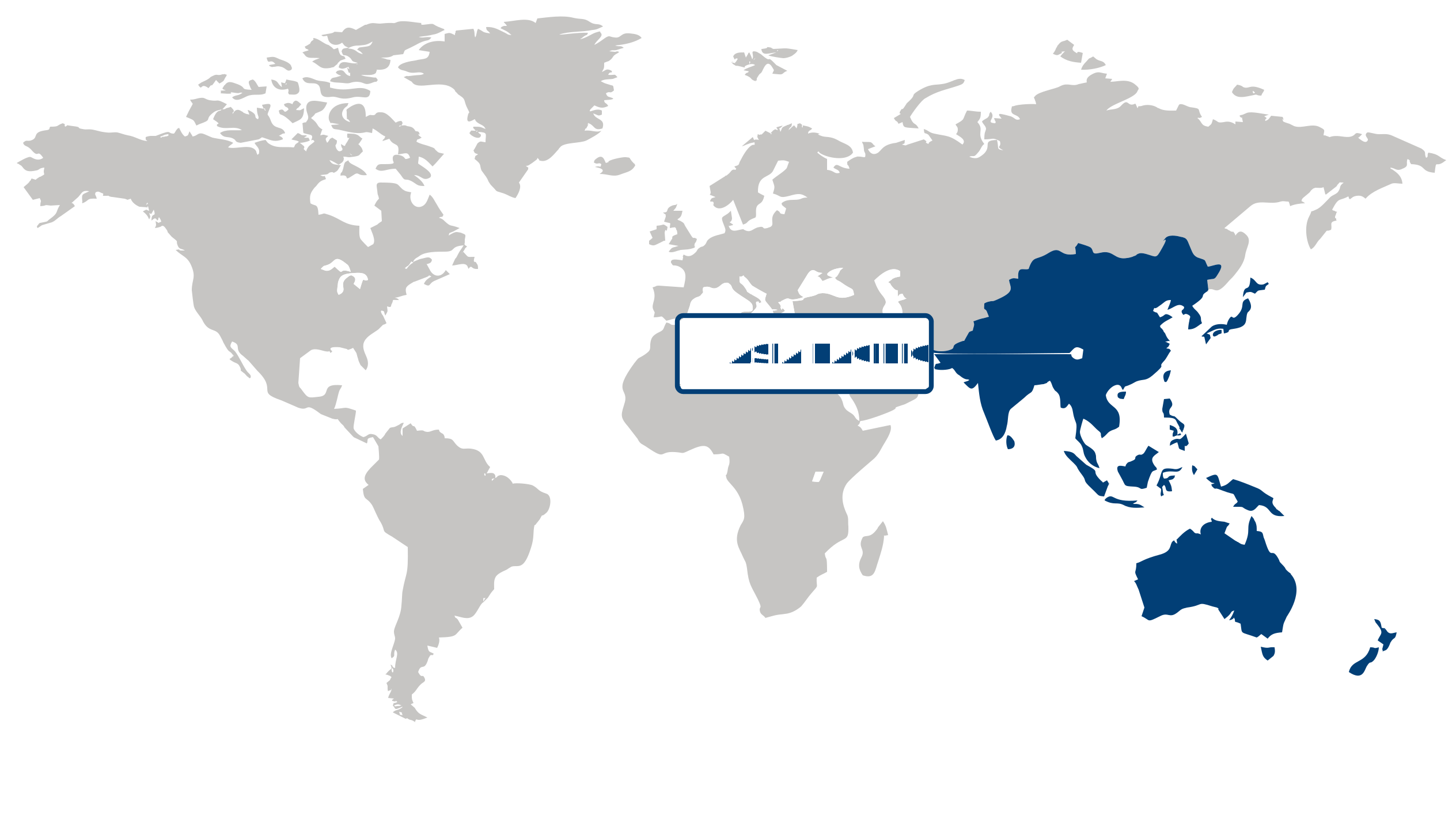
Asia Pacific (Largest Region)
Asia Pacific held the largest share of the 3D stacking market in 2026, led by strong semiconductor manufacturing capabilities, expanding investments in advanced packaging technologies, and growing demand for high-performance computing components. The region’s established electronics and semiconductor ecosystem is encouraging the adoption of 3D stacking technologies to improve computing performance, integration density, and energy efficiency. Increasing demand for advanced processors, memory solutions, and compact electronic architectures is further driving investment in vertically integrated semiconductor designs. In addition, the expansion of artificial intelligence, consumer electronics, data centers, and automotive electronics is creating favorable conditions for broader deployment of 3D stacking technologies across the regional semiconductor industry.
North America (Fastest-Growing Region)
North America is expected to register the fastest growth in the 3D stacking market, influenced by increasing investment in advanced semiconductor architectures, artificial intelligence infrastructure, and high-performance computing. Growing demand for enhanced processing capabilities and greater chip integration is encouraging the development of vertically stacked semiconductor solutions. The region’s strong research and development ecosystem and increasing focus on next-generation computing technologies are supporting advancements in advanced packaging and heterogeneous integration. Rising demand for energy-efficient and high-density computing systems is further accelerating the adoption of 3D stacking technologies across data-intensive applications.
| Parameter | North America | Asia Pacific | Europe | Latin America | MEA |
|---|---|---|---|---|---|
| Innovation HubiScaleNascentDeveloping Advanced | |||||
| Cost-Sensitive RegioniScaleLowMedium High | |||||
| Regulatory EnvironmentiScaleRestrictiveNeutral Supportive | |||||
| Demand DriversiScaleWeakModerate Strong | |||||
| Development StageiScaleEmergingDeveloping Developed | |||||
| Adoption RateiScaleLowMedium High | |||||
| New Entrants / StartupsiScaleSparseModerate Dense | |||||
| Macro IndicatorsiScaleWeakStable Strong |
Key Country Insights
United States 🇺🇸
Advanced Chip IntegrationThe U.S. 3D stacking market is strongly connected to advanced semiconductor architectures requiring greater computing performance and integration within constrained footprints. Commercial priorities include high-bandwidth interconnects, thermal management, manufacturing yield, and integration of stacked components into sophisticated computing platforms.
Germany 🇩🇪
Automotive Semiconductor IntegrationGermany's 3D stacking market has relevance across automotive electronics, industrial systems, and high-performance semiconductor applications. Priorities center on reliable stacked architectures, thermal control, manufacturing quality, and integration into electronics requiring greater functionality without proportional increases in physical size.
Japan 🇯🇵
High-Density Packaging ExpertiseJapan's 3D stacking market is closely associated with advanced semiconductor packaging, memory, electronics, and precision manufacturing capabilities. Market priorities include miniaturization, interconnect reliability, thermal performance, and efficient integration of multiple functional layers within compact electronic devices.
South Korea 🇰🇷
Memory Stacking ExpansionSouth Korea's 3D stacking market is closely tied to advanced memory and semiconductor manufacturing, where stacking supports higher functionality and bandwidth. Commercial priorities include process precision, yield improvement, thermal management, and scalable manufacturing of increasingly complex stacked chip architectures.
France 🇫🇷
Research-Led Chip PackagingFrance's 3D stacking market is supported by advanced semiconductor research, electronics development, and specialized industrial applications. Priorities include reliable vertical integration, thermal management, packaging innovation, and translating advanced stacking techniques into commercially viable high-performance electronic systems.
Italy 🇮🇹
Specialized Packaging ApplicationsItaly's 3D stacking market is oriented toward specialized electronics, industrial applications, and semiconductor packaging requirements where compact integration offers practical benefits. Commercial priorities include manufacturing reliability, thermal performance, and cost-conscious adoption of advanced stacked architectures.
3D Stacking Market Share (%), by Interconnecting Technology, 2026
Go beyond the chart, access full insights & data tables
Request Free Sample ReportInterconnecting Technology Segment Analysis: 3D TSV (Through-Silicon Via) (Largest Segment) vs Monolithic 3D Integration (Fastest-Growing Segment)
The 3D TSV (through-silicon via) segment accounted for the largest revenue share of 46.96% in 2026, supported by its established role in enabling vertical electrical connections between stacked semiconductor dies. TSV technology facilitates high-density interconnections, shorter signal transmission paths, and improved communication between vertically integrated chips, making it particularly suitable for advanced memory architectures and high-performance computing applications. Its ability to support heterogeneous integration while maintaining electrical connectivity across multiple semiconductor layers has encouraged widespread adoption in applications requiring enhanced bandwidth and compact device configurations. Furthermore, the increasing demand for advanced memory solutions, high-speed data processing, and efficient semiconductor packaging is strengthening the relevance of TSV-based architectures. Established manufacturing capabilities and continued improvements in via formation, bonding, and integration processes are also supporting its commercial utilization. As semiconductor manufacturers increasingly pursue higher integration density and improved performance across compact footprints, 3D TSV technology continues to play a significant role in advancing three-dimensional semiconductor architectures.
The monolithic 3D integration segment is projected to register the fastest growth, driven by its potential to enable dense vertical integration through the sequential fabrication of semiconductor layers in a single integrated structure. Unlike conventional die-stacking approaches, monolithic integration allows different functional layers to be interconnected through fine-grained connections, supporting improved communication efficiency and reduced interconnect complexity. This architecture is gaining attention as semiconductor manufacturers seek innovative approaches to overcome limitations associated with conventional scaling and increasing transistor density. The growing requirement for compact, energy-efficient, and high-performance semiconductor devices is encouraging research and development into monolithic integration techniques. Additionally, advancements in low-temperature processing, transistor fabrication, and sequential layer integration are improving the feasibility of developing complex multi-layer semiconductor structures. Its potential applications in advanced logic, memory integration, and heterogeneous computing are creating opportunities for wider adoption as fabrication technologies mature.
Method Segment Analysis: Die-to-die (Largest Segment) vs Wafer-to-Wafer (Fastest-Growing Segment)
The die-to-die segment accounted for the largest revenue share of 42.82% in the 3D stacking method segment in 2026, driven by its flexibility in integrating separately fabricated semiconductor dies into vertically integrated architectures. This approach allows manufacturers to integrate different chip components based on their individual process requirements, enabling heterogeneous integration without requiring all functional layers to be fabricated using the same semiconductor process. Die-to-die stacking is particularly relevant for applications involving advanced processors, memory components, and specialized computing architectures where performance optimization and design flexibility are important considerations. Furthermore, the ability to select and integrate dies with different functionalities supports efficient utilization of semiconductor manufacturing capabilities. The growing demand for advanced packaging solutions that enhance processing performance, bandwidth, and integration density is reinforcing the adoption of die-to-die methods. Continued improvements in bonding technologies, alignment accuracy, and interconnect design are further strengthening their suitability for complex semiconductor packaging applications.
The wafer-to-wafer segment is expected to witness the fastest growth, supported by its potential to streamline semiconductor stacking through the direct bonding and integration of entire wafers. This method enables manufacturers to establish vertical connections across multiple semiconductor layers while supporting high-density integration and efficient interconnect formation. Its suitability for applications requiring uniform stacking and large-scale production is attracting increasing interest as demand for advanced semiconductor architectures expands. Additionally, wafer-to-wafer processing can support improved manufacturing throughput when the wafers involved have compatible dimensions and structural characteristics. The increasing development of wafer bonding techniques, advanced lithography, and precision alignment processes is helping address technical challenges associated with this integration approach. As semiconductor manufacturers pursue greater packaging efficiency, improved electrical performance, and scalable three-dimensional integration, wafer-to-wafer stacking is gaining relevance across advanced memory and logic applications.
Device Type Segment Analysis: Memory Devices (Largest Segment) vs Logic ICs (Fastest-Growing Segment)
The memory devices segment accounted for the largest revenue share of 32.83% in 2026, primarily driven by the increasing requirement for high-density memory architectures capable of supporting data-intensive computing applications. Three-dimensional stacking enables multiple memory layers to be integrated across a compact footprint, improving storage density and facilitating higher data transfer capabilities. These characteristics are particularly important for applications involving artificial intelligence, cloud computing, high-performance computing, and advanced data processing, where efficient memory access and bandwidth are essential. Furthermore, the growing volume of digital information generated through connected devices, enterprise applications, and intelligent computing systems is increasing demand for advanced memory technologies. Stacked memory architectures also provide opportunities to optimize space utilization and reduce interconnection distances, supporting improved system-level performance. Continuous advancements in memory fabrication, bonding processes, and high-density packaging are further strengthening the adoption of three-dimensional stacking across memory devices.
The logic ICs segment is projected to experience the fastest growth, supported by the increasing demand for advanced computing architectures that deliver higher processing performance, improved energy efficiency, and greater functional integration. Three-dimensional stacking allows logic components to be integrated with other semiconductor layers, supporting shorter interconnect pathways and improved communication between processing elements. This capability is becoming increasingly important in applications such as artificial intelligence accelerators, advanced processors, automotive electronics, and high-performance computing systems, where conventional planar architectures face growing integration challenges. Additionally, the expansion of complex semiconductor designs is encouraging manufacturers to explore vertical integration techniques that improve chip functionality without relying exclusively on traditional scaling methods. Advances in hybrid bonding, chiplet integration, and heterogeneous packaging are further creating opportunities for incorporating stacked logic structures into next-generation semiconductor devices. As demand for computationally intensive applications continues to expand, logic ICs are gaining importance in the evolving three-dimensional semiconductor integration landscape.
| Segment | Sub-Segment | Largest Segment | Fastest Growing |
|---|---|---|---|
| Interconnecting Technology | 3D Hybrid Bonding, 3D TSV (Through-Silicon Via), Monolithic 3D Integration | 3D TSV (Through-Silicon Via) | Monolithic 3D Integration |
| Method | Die-to-Die, Die-to-Wafer, Wafer-to-Wafer, Chip-to-Chip, Chip-to-Wafer | Die-to-die | Wafer-to-Wafer |
| Device Type | Logic ICs, Imaging & Optoelectronics, Memory Devices, MEMS/Sensors, LEDs, Others | Memory Devices | Logic ICs |
| End Use Industry | Consumer Electronics, Manufacturing, Communications, Automotive, Medical Devices/Healthcare, Others | Consumer Electronics | Communications |
Unlock insights tailored to your business with our bespoke market research solutions.
Click to get your customized report now.
Competitive Landscape and Market Positioning
Analyst Perspective:
In 3D stacking, market differentiation centers on mastering high-density interconnect precision and advanced bonding reliability to maximize substrate yields across complex multi-die assemblies. As heterogeneous chiplet architectures gain traction—combining disparate memory, logic, and acceleration dies—suppliers face heightened manufacturing risks where single-interface defects invalidate entire packages. Addressing severe heat concentration within vertically stacked dies requires sophisticated thermal dissipation architectures that sustain performance without inflating total package volume. Ultimately, semiconductor packaging providers that successfully balance fine-pitch Through-Silicon Via (TSV) integration with flexible chiplet design options can capture high-performance computing demand while mitigating yield loss and design complexity.
Key companies in the 3D stacking market:
- TSMC (Taiwan)
- Intel Corporation (USA)
- Samsung Electronics (South Korea)
- AMD (USA)
- Micron Technology (USA)
- Broadcom (USA)
- SK Hynix (South Korea)
- ASE Technology Holding (Taiwan)
- Amkor Technology (USA)
- IBM (USA)
| Company | Market Share | Company Revenue | Revenue CAGR (%) | Product Portfolio | Geographic Presence | Innovation / R&D Focus | Strategic Developments |
|---|---|---|---|---|---|---|---|
| TSMC (Taiwan) | |||||||
| Intel Corporation (USA) | |||||||
| Samsung Electronics (South Korea) | |||||||
| AMD (USA) | |||||||
| Micron Technology (USA) | |||||||
| Broadcom (USA) | |||||||
| SK Hynix (South Korea) | |||||||
| ASE Technology Holding (Taiwan) | |||||||
| Amkor Technology (USA) | |||||||
| IBM (USA) |
Industry Development/News
| Company Name | Date | Key Development |
|---|---|---|
| Micron | March 2026 | Micron scheduled tool move-in at PSMC’s Tongluo P5 fab after signing an exclusive letter of intent to acquire the facility for US$1.8 billion. The transaction represents a major manufacturing and capacity expansion initiative that can strengthen Micron’s semiconductor production footprint and support advanced technology development. |
| Dreambig Semiconductor | January 2025 | Dreambig Semiconductor partnered with Samsung Foundry to develop the MARS chip label platform using Chiplet Hub and Networking IO chiplets. The collaboration leverages Samsung's SF4X FinFET process technology and advanced 3D chip-on-wafer stacking alongside HBM memory-synergistic packaging expertise. |
| Lightmatter | November 2024 | Lightmatter entered into a strategic partnership with Amkor Technology to deliver a 3D-packaged chip complex powered by Passage technology. The companies are developing a 3D-stacked photonic engine designed to meet AI workload demands through enhanced interconnect scaling and power management capabilities. |
| PSMC | November 2024 | PSMC partnered with AP Memory to launch a 3D AI Foundry strategy targeting the requirements of AI systems. The initiative combines foundry and memory-related capabilities around three-dimensional integration, providing a strategic pathway for PSMC to expand its participation in AI-oriented semiconductor architectures and advanced packaging applications. |
| Intel | January 2024 | Intel opened an advanced packaging fab in New Mexico as part of its expansion of local semiconductor manufacturing operations. The facility development strengthens Intel’s advanced packaging footprint and supports the company’s broader efforts to develop increasingly sophisticated semiconductor integration technologies, including architectures involving stacked and multi-die components. |
Customize Your Report
Explore examples of how this report can be tailored to different research needs, including custom segments, additional topics or chapters, and related reports. Click a section of the wheel or its numbered marker to explore the available options.
3D Stacking Market — Custom Segments
| Segment | Sub-Segment |
|---|---|
| Semiconductor Process Node | Mature nodes, 16–28 nm nodes, 7–14 nm nodes, 5 nm and below |
| Supply Chain Participant | Semiconductor manufacturers, OSAT providers, Foundries, Integrated device manufacturers, Equipment and materials suppliers |
| Production Volume | Low-volume production, Medium-volume production, High-volume production |
3D Stacking Market — Custom TOC
| Custom Chapter | Chapter Details |
|---|---|
| 3D Integration Adoption Roadmap |
|
| Thermal Management Strategy |
|
| Chiplet & Heterogeneous Integration Outlook |
|
Need a different cut of the data?
Request Custom ResearchFrequently Asked Questions
How much revenue does the 3D stacking market generate?
How will the 3D stacking industry grow in terms of size and CAGR by 2036?
How is advanced semiconductor packaging accelerating adoption of 3D stacking?
Why are high-density interconnect innovations becoming strategically important for 3D stacking?
Which interconnecting technology held the largest share of the 3D stacking market in 2026?
Which device type is projected to grow fastest in the 3D stacking market?
Why is Asia Pacific the leading market for 3D stacking technologies?
What is accelerating 3D stacking market growth in North America?
What are the prominent companies operating in the 3D stacking landscape?
Our Clients
"Working with FBI has been a good experience. The market report provided a holistic view, covering everything from emerging trends to potential risks."
Semtech Corporation
"The experience was highly positive. The team showcased remarkable flexibility in adapting to our specific needs and delivered report that perfectly aligned with all our requirements."
TSMC
"What really stood out to me was how clearly and promptly the Fundamental Business Insights team communicated throughout. It made the collaboration feel effortless."
NXP Semiconductors
Our Research Team & Methodology
Every Fundamental Business Insights report is built by a dedicated vertical research team, validated through a structured primary-and-secondary methodology, and reviewed for accuracy before it reaches you.
This report was prepared by the Electronics & Semiconductors Research Team at Fundamental Business Insights, a dedicated research group specializing in the global electronics and semiconductor ecosystem. Our analysts continuously monitor technology innovations, manufacturing trends, competitive developments, supply chain dynamics, regulatory changes, and end-user demand to deliver timely market intelligence. The research is developed using a structured methodology that combines primary industry interactions, company financial disclosures, government publications, trade associations, technical literature, patent analysis, and other authoritative secondary sources. Market estimates are validated through multiple research techniques, including top-down and bottom-up analysis, before undergoing an internal quality review to ensure accuracy, consistency, and methodological integrity prior to publication.
Delivery
Published
Available
Support
- Market Size & Forecast
- Market Segmentation
- Regional Analysis
- Growth Drivers & Challenges
- Market Dynamics
- Competitive Landscape
- Company Profiles
- Competitive Benchmarking
- Mergers & Acquisitions
- Market Share Analysis or Key Company Strategies
- Value Chain Analysis
- Porter's Five Forces
- PESTLE Analysis
- Pricing Trends
- Supply-Demand Analysis
- Technology Landscape
- Regulatory Landscape
- Investment & Funding Landscape
- Emerging Opportunities
- Future Market Outlook