Advanced IC Substrates Market Size & Growth Forecast 2027–2036, By Segments (Type, Technology, Application), Regional Demand Trends (North America, Asia Pacific, Europe), Key Country Insights (U.S., Japan, South Korea, Germany, France, Italy), and Competitive Landscape
Jump to Content
Market Size and Growth Outlook
Advanced IC Substrates Market size was more than USD 19.51 billion in 2026 and is set to grow at a 9.96% CAGR between 2027 and 2036, reaching USD 50.42 billion by 2036. The industry revenue for 2027 is assessed at USD 21.16 billion.
Get more details on this report
Request Free Sample ReportAdvanced IC Substrates Market Intelligence Snapshot
Regional Market Dynamics
- Asia Pacific leads through its extensive semiconductor manufacturing ecosystem, electronics production base, and investments in advanced packaging, supporting demand for reliable substrates used in high-performance electronic devices.
- Semiconductor manufacturing investments, advanced packaging development, domestic capacity expansion, and demand from AI and high-performance computing are increasing opportunities for advanced IC substrates.
Segment Momentum
- FCBGA substrates held a 39.42% market share in 2026, driven by demand for high-performance semiconductor packaging, efficient electrical connectivity, thermal management, and higher I/O density in computing, graphics, and networking applications.
- HDI substrates are gaining momentum through finer circuit patterns, higher component density, and compact interconnections. Their growing use across mobile electronics, computing, and automotive electronics supports manufacturers' miniaturization and performance priorities.
Market Expansion Drivers
- Advanced substrate demand in ICs.
- High-density interconnect substrates.
- Next-gen packaging architectures.
Leading Market Participants
- Major companies in the advanced IC substrates market include Ibiden (Japan), Unimicron (Taiwan), Shinko Electric (Japan), Samsung Electro-Mechanics (South Korea), ASE Technology (Taiwan), AT&S (Austria), Kinsus Interconnect Technology (Taiwan), Nan Ya PCB (Taiwan), TTM Technologies (USA), LG Innotek (South Korea).
Global Market Forecast Snapshot
Market Outlook
- 2026 Market Size: USD 19.51 billion
- 2027 Estimated Market Size: USD 21.16 billion
- Projected Market Size: USD 50.42 billion by 2036
- Growth Forecast: 9.96% CAGR (2027-2036)
Regional and Segment Outlook
- Leading Regional Market: Asia Pacific
- High-Growth Regional Hub: North America
- Core Revenue Segment: Type (Flip Chip Ball Grid Array (FCBGA) Substrates) | Technology (High-Density Interconnect (HDI) Substrates) | Application (Mobile and Consumer Electronics)
- Emerging Opportunity Segment: Type (Flip Chip Ball Grid Array (FCBGA) Substrates) | Technology (High-Density Interconnect (HDI) Substrates) | Application (Mobile and Consumer Electronics)
Market Growth Drivers and Industry Trends
Advanced substrate demand in ICs
The increasing complexity of integrated circuits is driving demand for advanced substrates capable of supporting higher performance, greater component density, and improved electrical connectivity. As electronic devices incorporate more sophisticated computing and processing capabilities, substrates must provide enhanced support for increasingly complex chip designs. This evolution in integrated circuit architecture is strengthening the need for advanced substrate technologies across electronics applications.
High-density interconnect substrates
The growing requirement for compact and high-performance electronic systems is increasing the adoption of high-density interconnect substrates. These substrates enable manufacturers to accommodate complex circuit configurations within smaller form factors while supporting efficient signal transmission and component integration. The continued miniaturization of electronic devices and rising demand for higher functionality are therefore creating favorable conditions for market expansion.
Next-gen packaging architectures
The development of advanced semiconductor packaging architectures is increasing the need for substrate technologies that can support greater integration and improved system performance. Emerging packaging approaches require substrates capable of handling complex interconnections, enhanced thermal requirements, and tighter component arrangements. As semiconductor manufacturers adopt more sophisticated packaging designs to address evolving performance requirements, demand for advanced IC substrates is expected to grow.
| Growth Driver | Impact on CAGR | Regulatory Influence | Geographic Relevance | Adoption Rate | Impact Timeline |
|---|---|---|---|---|---|
| Advanced substrate demand in ICs | 2.8% | Short term (≤ 2 yrs) | Asia Pacific; Europe | Medium | Moderate |
| High-density interconnect substrates | 2.2% | Medium term (2–5 yrs) | Europe; North America | Medium | Moderate |
| Next-gen packaging architectures | 1.6% | Long term (5+ yrs) | Asia Pacific; Europe | Medium | Slow |
Explore Growth Opportunities
Request Free Sample ReportRegional Demand Dynamics
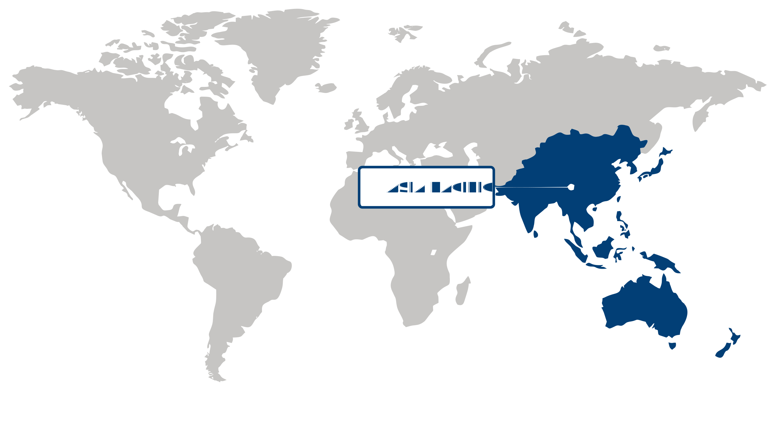
Asia Pacific (Largest Region)
Asia Pacific held the largest share of the advanced IC substrates market in 2026, supported by its strong semiconductor manufacturing ecosystem, extensive electronics production base, and growing demand for advanced computing technologies. The region has established capabilities across semiconductor packaging, electronic components, and integrated circuit manufacturing, creating a favorable environment for advanced substrate adoption. Increasing production of high-performance electronic devices and growing demand for compact, efficient, and reliable semiconductor packages are strengthening market opportunities. In addition, continued investments in semiconductor manufacturing infrastructure and technological advancements in packaging are supporting the development of sophisticated substrate solutions across the region.
North America (Fastest-Growing Region)
North America is expected to register the fastest growth in the advanced IC substrates market, driven by increasing investments in semiconductor manufacturing, advanced packaging technologies, and high-performance computing infrastructure. Growing demand for sophisticated electronic systems used in computing, telecommunications, automotive applications, and other technology-intensive sectors is creating greater need for advanced substrate solutions. The expansion of domestic semiconductor capabilities and increasing focus on resilient supply chains are further encouraging investments across the semiconductor packaging ecosystem. Moreover, continued innovation in artificial intelligence, data processing, and next-generation electronic systems is supporting demand for advanced IC substrates with enhanced performance and reliability.
| Parameter | North America | Asia Pacific | Europe | Latin America | MEA |
|---|---|---|---|---|---|
| Innovation HubiScaleNascentDeveloping Advanced | |||||
| Cost-Sensitive RegioniScaleLowMedium High | |||||
| Regulatory EnvironmentiScaleRestrictiveNeutral Supportive | |||||
| Demand DriversiScaleWeakModerate Strong | |||||
| Development StageiScaleEmergingDeveloping Developed | |||||
| Adoption RateiScaleLowMedium High | |||||
| New Entrants / StartupsiScaleSparseModerate Dense | |||||
| Macro IndicatorsiScaleWeakStable Strong |
Key Country Insights
United States 🇺🇸
Advanced Packaging DemandThe U.S. advanced IC substrates market is supported by demand from high-performance computing, AI accelerators, networking, and advanced semiconductor packaging. Supply-chain resilience and domestic semiconductor investment are encouraging greater attention to high-density substrates, advanced packaging capabilities, and qualified suppliers for increasingly complex chip architectures.
Germany 🇩🇪
Automotive Substrate IntegrationGermany’s advanced IC substrates market is closely linked to automotive electronics, industrial systems, and high-reliability semiconductor applications. Substrate suppliers are prioritizing thermal performance, miniaturization, and dependable manufacturing processes as vehicle electrification, automated systems, and industrial computing increase packaging requirements for sophisticated electronic components.
Japan 🇯🇵
Substrate Manufacturing ExpertiseJapan’s advanced IC substrates market benefits from deep capabilities in semiconductor materials, packaging technologies, and precision manufacturing. Industry priorities center on high-density interconnects, fine-line substrates, and advanced packaging materials needed for AI, high-performance computing, memory, and increasingly compact electronic architectures.
South Korea 🇰🇷
High-Density Packaging FocusSouth Korea’s advanced IC substrates market is strongly connected to memory, AI computing, and advanced semiconductor packaging requirements. Manufacturers are concentrating on fine-line, high-layer-count, and high-performance substrates that support increasingly demanding chip designs while strengthening integration between substrate production and major semiconductor manufacturing ecosystems.
France 🇫🇷
Aerospace Semiconductor ReliabilityFrance’s advanced IC substrates market is influenced by demanding aerospace, defense, telecommunications, and industrial electronics applications where reliability and thermal performance are critical. Suppliers are prioritizing specialized substrate technologies, high-reliability materials, and secure sourcing for complex semiconductor packages used in mission-critical electronic systems.
Italy 🇮🇹
Industrial Electronics ApplicationsItaly’s advanced IC substrates market is supported by industrial automation, automotive electronics, telecommunications, and specialized electronic equipment. Market priorities include compact and thermally efficient substrate solutions, manufacturing flexibility, and dependable component supply for increasingly sophisticated electronic assemblies used across industrial and mobility applications.
Advanced IC Substrates Market Share (%), by Type, 2026
Go beyond the chart, access full insights & data tables
Request Free Sample ReportType Segment Analysis: Flip Chip Ball Grid Array (FCBGA) Substrates (Largest & Fastest-Growing Segment)
The flip chip ball grid array (FCBGA) substrates segment accounted for a 39.42% share of the advanced IC substrates market in 2026, supported by its increasing adoption in high-performance semiconductor applications that require efficient electrical connectivity, enhanced signal integrity, and effective thermal management. FCBGA substrates provide a compact interconnection structure that supports the integration of complex and high-density semiconductor packages, making them well suited for processors, graphics solutions, networking components, and other advanced electronic devices. The growing demand for higher computing performance and increasingly sophisticated chip architectures is encouraging semiconductor manufacturers to adopt advanced packaging technologies, strengthening demand for FCBGA substrates. In addition, continued development of artificial intelligence, high-performance computing, data-intensive applications, and advanced consumer electronics is creating greater requirements for substrates capable of supporting higher I/O density and improved package performance. These factors are reinforcing the position of FCBGA substrates while supporting their rapid share growth in 2026 as semiconductor packaging continues to evolve toward greater miniaturization, performance, and integration.
Technology Segment Analysis: High-Density Interconnect (HDI) Substrates (Largest & Fastest-Growing Segment)
The high-density interconnect (HDI) substrates segment is the leading category in share for 2026 and represents the fastest-growing technology segment, driven by the increasing need for compact, high-density, and reliable interconnection solutions in advanced electronic devices. HDI technology enables finer circuit patterns, improved routing capabilities, and greater component density within constrained package dimensions, making it particularly suitable for applications where miniaturization and performance are critical. The continued development of sophisticated semiconductor devices is increasing the complexity of interconnections, encouraging manufacturers to adopt HDI substrates to accommodate higher circuit density while maintaining efficient electrical performance. Growing adoption across mobile electronics, computing systems, automotive electronics, and other advanced applications is further supporting demand in the advanced IC substrates market. Moreover, ongoing advancements in semiconductor packaging and the shift toward smaller and more integrated electronic architectures are creating favorable conditions for HDI technology, strengthening its role as a key technology.
Application Segment Analysis: Mobile and Consumer Electronics (Largest & Fastest-Growing Segment)
The mobile and consumer electronics segment represents the leading 2026 share and fastest-growing application segment, supported by the continued integration of increasingly sophisticated semiconductor components into smartphones, tablets, wearable devices, computing products, and other connected electronics. Consumers' demand for thinner, faster, more powerful, and feature-rich electronic devices is encouraging manufacturers to adopt advanced semiconductor packaging solutions that provide higher functionality within compact form factors. Advanced IC substrates are particularly important in these applications because they facilitate efficient electrical interconnections while supporting miniaturization, high component density, and improved device performance. The expansion of connected devices and the growing incorporation of artificial intelligence, high-speed processing, advanced imaging, and connectivity features are further increasing the complexity of electronic architectures. In addition, rapid product development cycles and continuous innovation in consumer electronics are encouraging greater adoption of advanced packaging technologies, supporting sustained demand in the advanced IC substrates market for mobile and consumer applications.
| Segment | Sub-Segment | Largest Segment | Fastest Growing |
|---|---|---|---|
| Type | Flip Chip Ball Grid Array (FCBGA) Substrates, Flip Chip Chip Scale Package (FCCSP) Substrates, Wire Bond Substrates, Embedded Substrates, Others | Flip Chip Ball Grid Array (FCBGA) Substrates | Flip Chip Ball Grid Array (FCBGA) Substrates |
| Technology | High-Density Interconnect (HDI) Substrates, Build-Up Substrates, Coreless Substrates, Organic Substrates, Ceramic Substrates | High-Density Interconnect (HDI) Substrates | High-Density Interconnect (HDI) Substrates |
| Application | Mobile and Consumer Electronics, Automotive Electronics, Networking and Communication Devices, Computing and Data Centers, Others | Mobile and Consumer Electronics | Mobile and Consumer Electronics |
Unlock insights tailored to your business with our bespoke market research solutions.
Click to get your customized report now.
Competitive Landscape and Market Positioning
Analyst Perspective:
As semiconductor architectures transition to ultra-compact footprints, advanced IC substrate manufacturers are advancing coreless substrate precision and high-density interconnect scaling to handle intensive signal routing without compromising yield. To support high-volume, high-density packaging, suppliers are deploying fine-pitch wire bonding alongside advanced thermal dissipation materials to effectively manage localized heat generation in high-performance computing components. Ultimately, suppliers that master layer alignment, minimize warpage in ultra-thin form factors, and maintain rigorous thermal-mechanical stability will lead the next generation of semiconductor packaging.
Top players in the advanced IC substrates market:
- Ibiden (Japan)
- Unimicron (Taiwan)
- Shinko Electric (Japan)
- Samsung Electro-Mechanics (South Korea)
- ASE Technology (Taiwan)
- AT&S (Austria)
- Kinsus Interconnect Technology (Taiwan)
- Nan Ya PCB (Taiwan)
- TTM Technologies (USA)
- LG Innotek (South Korea)
| Company | Market Share | Company Revenue | Revenue CAGR (%) | Product Portfolio | Geographic Presence | Innovation / R&D Focus | Strategic Developments |
|---|---|---|---|---|---|---|---|
| Ibiden (Japan) | |||||||
| Unimicron (Taiwan) | |||||||
| Shinko Electric (Japan) | |||||||
| Samsung Electro-Mechanics (South Korea) | |||||||
| ASE Technology (Taiwan) | |||||||
| AT&S (Austria) | |||||||
| Kinsus Interconnect Technology (Taiwan) | |||||||
| Nan Ya PCB (Taiwan) | |||||||
| TTM Technologies (USA) | |||||||
| LG Innotek (South Korea) |
Industry Development/News
| Company Name | Date | Key Development |
|---|---|---|
| Advanced Chip and Circuit Materials (ACCM) | July 2026 | Advanced Chip and Circuit Materials introduced Celeritas SMC, a production-ready silicon-matched core for advanced IC substrates. The proprietary material matches silicon's thermal expansion coefficient while remaining compatible with established organic-substrate manufacturing workflows, facilitating advanced packaging applications without requiring fundamental process redesigns. |
| AT&S Malaysia | June 2026 | AT&S announced an expansion of its Kulim facility, featuring the fit-out of Plant 2 and new construction dedicated to IC substrate cores and advanced PCBs. Backed by agreements with AMD and a leading technology partner, the project expands contracted AI-oriented manufacturing capacity and deepens supply chain integration within Southeast Asia. |
| Ibiden | February 2026 | Ibiden announced a JPY 500 billion capital investment plan for its electronics business through fiscal years 2026 to 2028, allocating approximately JPY 280 billion to the Ohno Plant. This strategic funding scales high-performance IC package substrate capacity to support growing demand from AI server and accelerator ecosystems requiring premium FC-BGA substrates. |
| Ibiden | October 2025 | Ibiden held an opening ceremony for its Ohno Plant in Gifu Prefecture, establishing the site as a core production hub for AI server IC package substrates. Bringing the specialized facility online broadens the company's manufacturing base for high-value substrate classes and accelerates customer qualification timelines. |
| LG Chem | September 2025 | LG Chem completed the development of a proprietary high-resolution liquid PID material targeted at AI and high-performance semiconductor manufacturing. This commercialization effort expands the company's advanced materials portfolio to meet the rigorous packaging requirements associated with next-generation chip architectures. |
| AT&S Malaysia | July 2025 | AT&S Malaysia secured a US$150 million sustainability-linked loan from Maybank, marking a prominent regional financing arrangement. The facility provides capital to support broader operational activities and manufacturing footprint development within the advanced semiconductor substrate ecosystem in Southeast Asia. |
| AT&S Malaysia | March 2025 | AT&S secured a USD 250 million sustainability-linked loan from the International Finance Corporation to fund its modern IC substrate plant in Kulim, Malaysia. The financing aligns with emission reduction targets and expands production capacity to support advanced data-center processors for key customers like AMD. |
| ASE Group | February 2025 | ASE Group inaugurated its fifth chip packaging and testing facility in Penang, Malaysia, expanding its operational footprint to 3.4 million square feet. The plant integrates AIoT-driven automation for yield optimization and environmental sensing, enhancing global manufacturing capacity for generative AI, electric vehicle, and autonomous driving applications. |
Customize Your Report
Explore examples of how this report can be tailored to different research needs, including custom segments, additional topics or chapters, and related reports. Click a section of the wheel or its numbered marker to explore the available options.
Advanced IC Substrates Market — Custom Segments
| Segment | Sub-Segment |
|---|---|
| Substrate Size | Small-Size Substrates, Medium-Size Substrates, Large-Size Substrates |
| Manufacturing Process | Semi-Additive Process (SAP), Modified Semi-Additive Process (mSAP), Subtractive Process |
| Performance Grade | Standard-Performance Substrates, High-Performance Substrates, Ultra-High-Performance Substrates |
Advanced IC Substrates Market — Custom TOC
| Custom Chapter | Chapter Details |
|---|---|
| Substrate Supply Security Assessment |
|
| Capacity Expansion & Fab Investment Outlook |
|
| Foundry–OSAT–Substrate Ecosystem Dynamics |
|
Need a different cut of the data?
Request Custom ResearchFrequently Asked Questions
What is the market size of the advanced IC substrates market?
How is the advanced IC substrates industry expected to grow over the next 10 years?
How is increasing integrated circuit complexity driving demand in the advanced IC substrates market?
Why are high-density interconnects and next-generation packaging strengthening the strategic importance of advanced IC substrates?
Why do FCBGA substrates lead the advanced IC substrates market?
How is HDI substrate technology influencing purchasing decisions in the advanced IC substrates market?
Why does Asia Pacific lead the advanced IC substrates market?
What is driving the fastest growth in North America's advanced IC substrates market?
Who are the leading players in the advanced IC substrates landscape?
Our Clients
"Working with FBI has been a good experience. The market report provided a holistic view, covering everything from emerging trends to potential risks."
Semtech Corporation
"The experience was highly positive. The team showcased remarkable flexibility in adapting to our specific needs and delivered report that perfectly aligned with all our requirements."
TSMC
"What really stood out to me was how clearly and promptly the Fundamental Business Insights team communicated throughout. It made the collaboration feel effortless."
NXP Semiconductors
Our Research Team & Methodology
Every Fundamental Business Insights report is built by a dedicated vertical research team, validated through a structured primary-and-secondary methodology, and reviewed for accuracy before it reaches you.
This report was prepared by the Electronics & Semiconductors Research Team at Fundamental Business Insights, a dedicated research group specializing in the global electronics and semiconductor ecosystem. Our analysts continuously monitor technology innovations, manufacturing trends, competitive developments, supply chain dynamics, regulatory changes, and end-user demand to deliver timely market intelligence. The research is developed using a structured methodology that combines primary industry interactions, company financial disclosures, government publications, trade associations, technical literature, patent analysis, and other authoritative secondary sources. Market estimates are validated through multiple research techniques, including top-down and bottom-up analysis, before undergoing an internal quality review to ensure accuracy, consistency, and methodological integrity prior to publication.
Delivery
Published
Available
Support
- Market Size & Forecast
- Market Segmentation
- Regional Analysis
- Growth Drivers & Challenges
- Market Dynamics
- Competitive Landscape
- Company Profiles
- Competitive Benchmarking
- Mergers & Acquisitions
- Market Share Analysis or Key Company Strategies
- Value Chain Analysis
- Porter's Five Forces
- PESTLE Analysis
- Pricing Trends
- Supply-Demand Analysis
- Technology Landscape
- Regulatory Landscape
- Investment & Funding Landscape
- Emerging Opportunities
- Future Market Outlook