Die Bonder Equipment Market Size & Growth Forecast 2027–2036, By Segments (Type, Bonding Technique, Application), Regional Demand Trends (North America, Asia Pacific, Europe), Key Country Insights (U.S., Japan, South Korea, Germany, France, Italy), and Competitive Landscape
Jump to Content
Market Size and Growth Outlook
Die Bonder Equipment Market size stood at USD 1.96 billion in 2026 and is predicted to grow at a 4.21% CAGR from 2027 to 2036, crossing USD 2.96 billion by 2036. The industry revenue for 2027 is assessed at USD 2.03 billion.
Get more details on this report
Request Free Sample ReportDie Bonder Equipment Market Intelligence Snapshot
Regional Market Dynamics
- Asia Pacific holds a 50.88% share, supported by its semiconductor manufacturing ecosystem, electronics production capacity, and investment in advanced packaging and precision assembly equipment.
- North America is gaining momentum through semiconductor supply chain localization, domestic manufacturing investment, and expanding advanced packaging capabilities, increasing demand for high-precision die bonding equipment.
Segment Momentum
- Automatic die bonders accounted for 49.82% of the market in 2026, supported by precise die placement, consistent bonding quality, and reduced manual intervention. Their capabilities help semiconductor manufacturers improve throughput and minimize assembly defects.
- Consumer electronics accounted for 39.2% of the market in 2026, driven by semiconductor demand across smartphones, laptops, wearables, and connected devices. Increasing miniaturization and high-density packaging requirements strengthen demand for precision die bonding equipment.
Market Expansion Drivers
- Rising demand for advanced die bonding in semiconductor production.
- Technological advancements in die bonder equipment.
- Expansion of semiconductor manufacturing in emerging economies.
Leading Market Participants
- Prominent players in the die bonder equipment market include ASM Pacific Technology (Hong Kong), Kulicke & Soffa (USA), Besi (Netherlands), Tokyo Electron (Japan), Panasonic (Japan), Hanmi Semiconductor (South Korea), Shinkawa (Japan), Palomar Technologies (USA), Toray Engineering (Japan), SET Corporation (France).
Global Market Forecast Snapshot
Market Outlook
- 2026 Market Size: USD 1.96 billion
- 2027 Estimated Market Size: USD 2.03 billion
- Projected Market Size: USD 2.96 billion by 2036
- Growth Forecast: 4.21% CAGR (2027-2036)
Regional and Segment Outlook
- Leading Regional Market: Asia Pacific
- High-Growth Regional Hub: North America
- Core Revenue Segment: Type (Automatic Die Bonders) | Bonding Technique (Epoxy) | Application (Consumer Electronics)
- Emerging Opportunity Segment: Type (Automatic Die Bonders) | Bonding Technique (Epoxy) | Application (Consumer Electronics)
Market Growth Drivers and Industry Trends
Rising Demand for Advanced Die Bonding in Semiconductor Production
Growing demand for sophisticated semiconductor devices is driving the need for advanced die bonding technologies that provide precision, reliability, and efficient assembly performance. Increasing complexity in chip architectures, miniaturization requirements, and demand for high-performance electronic components are encouraging semiconductor manufacturers to adopt advanced bonding processes capable of supporting demanding packaging and assembly applications.
Technological Advancements in Die Bonder Equipment
Continuous advancements in die bonder equipment are improving placement accuracy, bonding consistency, process automation, and compatibility with increasingly complex semiconductor packages. Innovations in equipment control, precision handling, and automated inspection are enabling manufacturers to improve production efficiency while supporting advanced packaging formats and increasingly stringent quality requirements.
Expansion of Semiconductor Manufacturing in Emerging Economies
The expansion of semiconductor manufacturing capabilities in emerging economies is creating additional demand for die bonding equipment as new fabrication, assembly, and packaging facilities are developed. Investments in local electronics production, supply chain diversification, and advanced manufacturing infrastructure are encouraging the deployment of modern semiconductor assembly technologies and supporting the broader adoption of automated die bonding solutions.
| Growth Driver | Impact on CAGR | Regulatory Influence | Geographic Relevance | Adoption Rate | Impact Timeline |
|---|---|---|---|---|---|
| Rising demand for advanced die bonding in semiconductor production | 1.5% | Short term (≤ 2 yrs) | Asia Pacific; North America; spillover: Europe | Medium | Fast |
| Technological advancements in die bonder equipment | 1.2% | Medium term (2–5 yrs) | North America; Europe; spillover: Asia Pacific | Medium | Moderate |
| Expansion of semiconductor manufacturing in emerging economies | 1% | Long term (5+ yrs) | Asia Pacific; Latin America; spillover: MEA | Low | Moderate |
Explore Growth Opportunities
Request Free Sample ReportRegional Demand Dynamics
Asia Pacific (Largest Region)
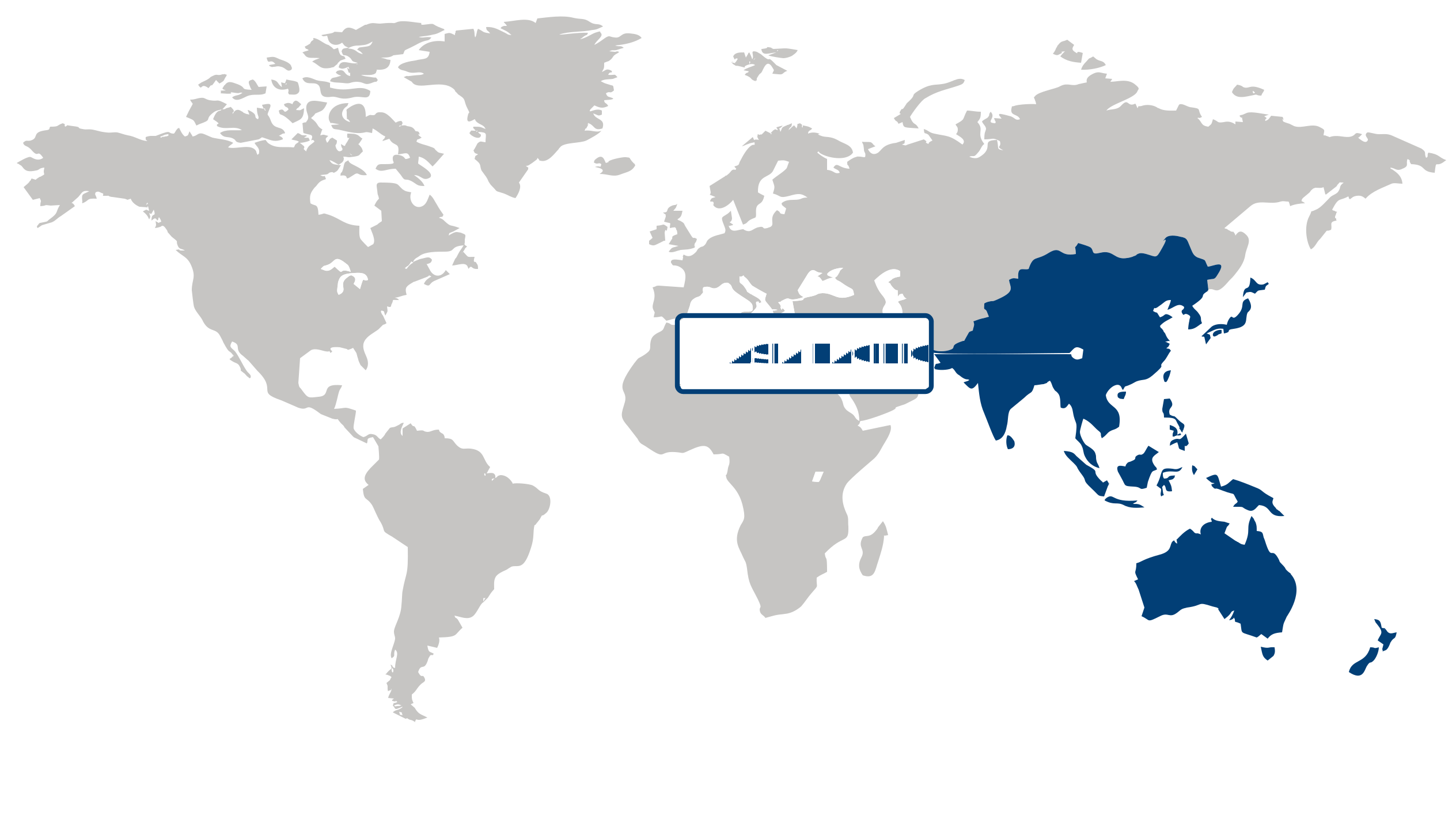
Asia Pacific accounted for a 50.88% share in 2026 and held the largest position in the die bonder equipment market, supported by a strong semiconductor manufacturing ecosystem, expanding electronics production, and increasing investments in advanced packaging technologies. The region benefits from extensive semiconductor fabrication and assembly capabilities, along with growing demand for electronic components used in consumer electronics, automotive systems, communications equipment, and industrial applications. Increasing adoption of advanced semiconductor packages and miniaturized electronic devices is driving demand for precise die bonding equipment that can support higher manufacturing efficiency and quality. In addition, investments in semiconductor production capacity and ongoing development of advanced packaging infrastructure are strengthening regional demand. The expansion of applications involving power electronics, sensors, and high-performance semiconductor devices is also creating opportunities for advanced die bonding technologies.
North America (Fastest-Growing Region)
North America is expected to experience the fastest growth in the die bonder equipment market, propelled by increasing investments in semiconductor manufacturing, advanced packaging capabilities, and domestic electronics production. Growing efforts to strengthen regional semiconductor supply chains are encouraging investments in fabrication, assembly, testing, and packaging infrastructure, creating opportunities for die bonding equipment. The increasing use of sophisticated semiconductor devices across automotive, communications, aerospace, defense, and industrial applications is further supporting demand for high-precision equipment. In addition, growing emphasis on localized semiconductor production and technological advancement is encouraging the adoption of advanced manufacturing systems. Continued development of next-generation packaging technologies and increasing demand for efficient and reliable semiconductor assembly processes are expected to further support market expansion.
| Parameter | North America | Asia Pacific | Europe | Latin America | MEA |
|---|---|---|---|---|---|
| Innovation HubiScaleNascentDeveloping Advanced | |||||
| Cost-Sensitive RegioniScaleLowMedium High | |||||
| Regulatory EnvironmentiScaleRestrictiveNeutral Supportive | |||||
| Demand DriversiScaleWeakModerate Strong | |||||
| Development StageiScaleEmergingDeveloping Developed | |||||
| Adoption RateiScaleLowMedium High | |||||
| New Entrants / StartupsiScaleSparseModerate Dense | |||||
| Macro IndicatorsiScaleWeakStable Strong |
Key Country Insights
United States 🇺🇸
Advanced Packaging IntegrationThe U.S. die bonder equipment market is shaped by demand for advanced semiconductor packaging, heterogeneous integration, and high-precision assembly. Equipment suppliers need to support tighter placement accuracy, flexible production configurations, and integration with increasingly sophisticated packaging processes.
Germany 🇩🇪
Precision Industrial BondingGermany’s die bonder equipment priorities reflect its strong focus on precision manufacturing and specialized semiconductor applications. Buyers are likely to emphasize placement accuracy, process repeatability, automation, and equipment compatibility with demanding power electronics and industrial component production.
Japan 🇯🇵
High-Precision AssemblyJapan continues to prioritize die bonding equipment capable of supporting miniaturized, high-reliability semiconductor devices and demanding manufacturing processes. Equipment performance, placement precision, process stability, and compatibility with automated production lines are central considerations across advanced electronics applications.
South Korea 🇰🇷
High-Volume Die BondingSouth Korea’s die bonder equipment priorities are closely connected to semiconductor manufacturing scale and increasingly complex packaging requirements. Manufacturers value high-throughput systems with precise placement, automation capabilities, and process control that can support demanding production environments.
France 🇫🇷
Specialized Packaging EquipmentFrance’s die bonder equipment demand is oriented toward specialized semiconductor and advanced electronics applications where process precision and reliability are critical. Suppliers can differentiate through flexible equipment configurations, automation, and bonding capabilities suited to lower-volume, technically demanding production.
Italy 🇮🇹
Flexible Assembly SystemsItaly’s die bonder equipment market favors adaptable systems that can serve specialized electronics and industrial manufacturing applications. Equipment flexibility, ease of integration, precise placement, and efficient changeovers are practical priorities for manufacturers managing diverse component and production requirements.
Die Bonder Equipment Market Share (%), by Type, 2026
Go beyond the chart, access full insights & data tables
Request Free Sample ReportType Segment Analysis: Automatic Die Bonders (Largest & Fastest-Growing Segment)
The automatic die bonders segment dominated the die bonder equipment market with a 49.82% share in 2026, driven by the growing demand for precision, operational efficiency, and consistent bonding quality in semiconductor manufacturing and advanced packaging processes. Automatic die bonders enable accurate die placement, controlled bonding operations, and reduced manual intervention, making them essential for manufacturers seeking to improve production throughput and minimize assembly defects. Their ability to perform repetitive bonding tasks with high precision and repeatability supports their widespread adoption in semiconductor fabrication, integrated circuit assembly, and electronic component manufacturing. The increasing miniaturization of semiconductor devices and growing complexity of chip architectures are further strengthening demand for automated bonding equipment capable of handling delicate components and stringent placement requirements. Automatic die bonders also help manufacturers optimize production workflows, reduce labor dependency, and maintain consistent output quality across high-volume manufacturing environments. The integration of advanced vision systems, intelligent alignment technologies, and automated process monitoring is further enhancing equipment accuracy, reliability, and operational flexibility. The segment is expected to maintain its growth momentum as the expansion of semiconductor manufacturing, increasing adoption of advanced packaging technologies, and rising demand for high-performance electronic components encourage investments in sophisticated automated die bonding solutions.
Bonding Technique Segment Analysis: Epoxy (Largest & Fastest-Growing Segment)
The epoxy bonding technique segment accounted for the largest share of the die bonder equipment market, with a 36.18% share in 2026, supported by its strong adhesive properties, cost efficiency, and compatibility with a broad range of semiconductor packaging applications. Epoxy bonding provides reliable mechanical attachment, structural stability, and effective insulation, making it suitable for die attachment across various electronic components and semiconductor devices. Its versatility in accommodating different die sizes, substrate materials, and packaging configurations enables manufacturers to achieve consistent bonding performance while maintaining efficient production processes. The technique is widely used in semiconductor assembly applications where dependable adhesion, process flexibility, and manufacturing cost optimization are important considerations. Advancements in epoxy formulations, dispensing technologies, and curing processes are further improving bonding strength, thermal stability, and long-term reliability, supporting the technique's adoption in increasingly sophisticated electronic assemblies. The segment is also benefiting from the growing demand for compact semiconductor devices and advanced packaging solutions that require precise material application and reliable die attachment. As manufacturers continue to prioritize production efficiency, bonding consistency, and compatibility with automated assembly systems, epoxy bonding is expected to remain an important technique in die bonding operations, with continued material innovation supporting its expanding applications.
Application Segment Analysis: Consumer Electronics (Largest & Fastest-Growing Segment)
The consumer electronics segment dominated the die bonder equipment market with a 39.2% share in 2026, driven by the extensive use of semiconductor components in smartphones, laptops, wearable devices, smart home appliances, and other connected electronic products. The continuous evolution of consumer electronics toward compact designs, enhanced processing capabilities, and improved energy efficiency is increasing the need for precise and reliable die bonding processes. Die bonders play a critical role in attaching semiconductor chips to substrates and packages, ensuring mechanical stability, electrical performance, and consistent product quality. The growing integration of processors, memory chips, sensors, and power management components into consumer devices is further supporting demand for advanced die bonding equipment. Manufacturers are increasingly focusing on miniaturization, high-density packaging, and efficient assembly processes to accommodate increasingly sophisticated electronic architectures. Automatic die bonding technologies support these requirements by improving placement accuracy, reducing assembly errors, and enabling consistent high-volume production. The segment is expected to maintain strong growth as demand for connected devices, smart electronics, and advanced computing capabilities continues to expand. Furthermore, the increasing adoption of advanced semiconductor packaging, coupled with the need for reliable component integration and streamlined manufacturing operations, is encouraging investments in precision die bonding equipment for consumer electronics applications.
| Segment | Sub-Segment | Largest Segment | Fastest Growing |
|---|---|---|---|
| Type | Manual Die Bonders, Semiautomatic Die Bonders, Automatic Die Bonders | Automatic Die Bonders | Automatic Die Bonders |
| Bonding Technique | Epoxy, Eutectic, UV, Others | Epoxy | Epoxy |
| Application | Consumer Electronics, Automotive, Industrial, Telecommunications, Others | Consumer Electronics | Consumer Electronics |
Unlock insights tailored to your business with our bespoke market research solutions.
Click to get your customized report now.
Competitive Landscape and Market Positioning
Analyst Perspective:
Advanced semiconductor packaging places a premium on die bonders that sustain sub-micron placement accuracy without sacrificing alignment speed. Equipment providers differentiate themselves through thermal and laser bonding consistency, ensuring high yield and structural integrity across diverse chip architectures. Floor-space optimization and strict cleanroom compatibility remain pivotal, as footprint constraints directly affect manufacturing layout and throughput. Ultimately, commercial success relies on high-speed execution, minimal changeover downtime, and repeatable performance that aligns seamlessly with upstream and downstream packaging workflows.
Prominent players in the die bonder equipment market:
- ASM Pacific Technology (Hong Kong)
- Kulicke & Soffa (USA)
- Besi (Netherlands)
- Tokyo Electron (Japan)
- Panasonic (Japan)
- Hanmi Semiconductor (South Korea)
- Shinkawa (Japan)
- Palomar Technologies (USA)
- Toray Engineering (Japan)
- SET Corporation (France)
| Company | Market Share | Company Revenue | Revenue CAGR (%) | Product Portfolio | Geographic Presence | Innovation / R&D Focus | Strategic Developments |
|---|---|---|---|---|---|---|---|
| ASM Pacific Technology (Hong Kong) | |||||||
| Kulicke & Soffa (USA) | |||||||
| Besi (Netherlands) | |||||||
| Tokyo Electron (Japan) | |||||||
| Panasonic (Japan) | |||||||
| Hanmi Semiconductor (South Korea) | |||||||
| Shinkawa (Japan) | |||||||
| Palomar Technologies (USA) | |||||||
| Toray Engineering (Japan) | |||||||
| SET Corporation (France) |
Industry Development/News
| Company Name | Date | Key Development |
|---|---|---|
| Adeia | July 2024 | Adeia entered into a long-term license agreement with Hamamatsu Photonics covering hybrid bonding technologies, encompassing both wafer-to-wafer and die-to-wafer solutions. This agreement expands upon a prior development license focused on the transfer of DBI Ultra technology, strengthening intellectual property commercialization and technology adoption within advanced semiconductor packaging segments. |
| SK Hynix | April 2024 | SK Hynix announced a USD 3.87 billion capital investment to construct an advanced packaging fabrication and R&D facility in West Lafayette, Indiana. The facility incorporates an advanced semiconductor production line dedicated to next-generation high-bandwidth memory chips utilizing precise die bonder equipment for assembly, bolstering domestic manufacturing capabilities and the regional AI supply chain. |
| MRSI Systems | September 2023 | MRSI Systems, operating as part of the Mycronic Group, introduced the MRSI-705HF high-force die bonder. Built on the existing MRSI-705 platform, the model delivers an application force capacity of up to 500N and operational heating up to 400°C with a heated bond head, addressing targeted manufacturing requirements in power semiconductor sintering and advanced integrated circuit packaging. |
Customize Your Report
Explore examples of how this report can be tailored to different research needs, including custom segments, additional topics or chapters, and related reports. Click a section of the wheel or its numbered marker to explore the available options.
Die Bonder Equipment Market — Custom Segments
| Segment | Sub-Segment |
|---|---|
| Package Type | Leaded Packages, Ball Grid Array (BGA) Packages, Chip-Scale Packages (CSP), Multi-Chip Packages (MCP), System-in-Package (SiP), Advanced 2.5D/3D Packages |
| Manufacturing Role | Integrated Device Manufacturers (IDMs), Outsourced Semiconductor Assembly and Test (OSAT) Providers, Foundries, Semiconductor Packaging Specialists |
| Production Use Case | High-Volume Production, Low-Volume & Specialty Production, Prototyping & Development, Research & Pilot Production |
Die Bonder Equipment Market — Custom TOC
| Custom Chapter | Chapter Details |
|---|---|
| Advanced Packaging Capacity Investment Roadmap |
|
| Customer Qualification & Vendor Switching Dynamics |
|
| Die Bonder Lifecycle & Service Economics |
|
Need a different cut of the data?
Request Custom ResearchFrequently Asked Questions
What is the overall size of the die bonder equipment market?
What are the growth projections for the die bonder equipment industry?
How are increasingly complex semiconductor architectures influencing die bonder equipment requirements?
How are equipment automation and precision improvements reshaping semiconductor assembly investments?
Why do automatic die bonders dominate the die bonder equipment market?
How is consumer electronics driving demand for die bonder equipment?
How does Asia Pacific maintain its leadership in the die bonder equipment market?
Why is North America expected to be the fastest-growing die bonder equipment market?
Which companies are driving growth in the die bonder equipment landscape?
Our Clients
"Working with FBI has been a good experience. The market report provided a holistic view, covering everything from emerging trends to potential risks."
Semtech Corporation
"The experience was highly positive. The team showcased remarkable flexibility in adapting to our specific needs and delivered report that perfectly aligned with all our requirements."
TSMC
"What really stood out to me was how clearly and promptly the Fundamental Business Insights team communicated throughout. It made the collaboration feel effortless."
NXP Semiconductors
Our Research Team & Methodology
Every Fundamental Business Insights report is built by a dedicated vertical research team, validated through a structured primary-and-secondary methodology, and reviewed for accuracy before it reaches you.
This report was prepared by the Electronics & Semiconductors Research Team at Fundamental Business Insights, a dedicated research group specializing in the global electronics and semiconductor ecosystem. Our analysts continuously monitor technology innovations, manufacturing trends, competitive developments, supply chain dynamics, regulatory changes, and end-user demand to deliver timely market intelligence. The research is developed using a structured methodology that combines primary industry interactions, company financial disclosures, government publications, trade associations, technical literature, patent analysis, and other authoritative secondary sources. Market estimates are validated through multiple research techniques, including top-down and bottom-up analysis, before undergoing an internal quality review to ensure accuracy, consistency, and methodological integrity prior to publication.
Delivery
Published
Available
Support
- Market Size & Forecast
- Market Segmentation
- Regional Analysis
- Growth Drivers & Challenges
- Market Dynamics
- Competitive Landscape
- Company Profiles
- Competitive Benchmarking
- Mergers & Acquisitions
- Market Share Analysis or Key Company Strategies
- Value Chain Analysis
- Porter's Five Forces
- PESTLE Analysis
- Pricing Trends
- Supply-Demand Analysis
- Technology Landscape
- Regulatory Landscape
- Investment & Funding Landscape
- Emerging Opportunities
- Future Market Outlook