Laser Debonding Equipment Market Size & Growth Forecast 2027–2036, By Segments (Technology, Laser Type, Application), Regional Demand Trends (North America, Asia Pacific, Europe), Key Country Insights (U.S., Japan, South Korea, Germany, France, Italy), and Competitive Landscape
Jump to Content
Market Size and Growth Outlook
Laser Debonding Equipment Market size was estimated at USD 2.53 billion in 2026 and is projected to grow at a 6.89% CAGR from 2027 to 2036, reaching USD 4.93 billion by 2036. The industry revenue for 2027 is estimated at USD 2.68 billion.
Get more details on this report
Request Free Sample ReportLaser Debonding Equipment Market Intelligence Snapshot
Regional Market Dynamics
- North America accounts for 37.8% of the market in 2026, driven by advanced semiconductor manufacturing, established electronics infrastructure, and investments in advanced packaging and precision manufacturing technologies.
- Expanding semiconductor capacity, rising electronics production, and investments in advanced packaging facilities are accelerating adoption across Asia Pacific, creating opportunities for precision laser systems in wafer processing and device manufacturing.
Segment Momentum
- Laser ablation held a 48.55% market share in 2026, supported by precise bonding-layer removal and reduced mechanical stress on sensitive substrates. These capabilities are valuable in advanced semiconductor manufacturing, where wafer integrity and process consistency are critical.
- Semiconductor wafer debonding accounted for 55.93% of the market in 2026 and is also the fastest-growing application segment. Laser-based separation helps protect thin, fragile wafers during advanced packaging and processing, supporting consistent yields and reduced substrate damage.
Market Expansion Drivers
- Rising demand for orthodontic and dental procedures.
- Technological advancements in laser debonding equipment.
- Increasing adoption in emerging dental markets.
Leading Market Participants
- Key players in the laser debonding equipment market include EV Group (Austria), SUSS MicroTec (Germany), ASMPT (Singapore), DISCO Corporation (Japan), Tokyo Electron (Japan), KLA (US), Nikon (Japan), Canon (Japan), Applied Materials (US), Hanmi Semiconductor (South Korea).
Global Market Forecast Snapshot
Market Outlook
- 2026 Market Size: USD 2.53 billion
- 2027 Estimated Market Size: USD 2.68 billion
- Projected Market Size: USD 4.93 billion by 2036
- Growth Forecast: 6.89% CAGR (2027-2036)
Regional and Segment Outlook
- Leading Regional Market: North America
- High-Growth Regional Hub: Asia Pacific
- Core Revenue Segment: Technology (Laser Ablation) | Laser Type (Ultraviolet (UV) Laser) | Application (Semiconductor Wafer Debonding)
- Emerging Opportunity Segment: Technology (Laser Ablation) | Laser Type (Ultraviolet (UV) Laser) | Application (Semiconductor Wafer Debonding)
Market Growth Drivers and Industry Trends
Rising demand for orthodontic and dental procedures
The increasing demand for orthodontic and dental procedures is driving the adoption of laser debonding equipment as dental professionals seek efficient and patient-friendly methods for removing orthodontic attachments. Laser-based debonding can facilitate the removal of brackets and adhesive materials while helping minimize mechanical stress on tooth surfaces and surrounding tissues. Growing awareness of aesthetic dental treatments, orthodontic care, and minimally invasive procedures is encouraging dental practices to adopt advanced technologies that can improve treatment efficiency and patient comfort. As orthodontic treatment becomes increasingly accessible across different patient groups, demand for specialized debonding solutions is expected to support market growth.
Technological advancements in laser debonding equipment
Technological advancements in laser debonding equipment are contributing to market growth by improving treatment precision, operational efficiency, and safety during orthodontic procedures. Developments in laser wavelength control, energy management, targeting systems, and treatment customization are enabling dental professionals to apply laser energy more accurately to bonding materials. Enhanced equipment design can also support easier handling and integration into existing dental workflows, encouraging broader clinical adoption. As manufacturers continue to develop more precise and user-friendly laser systems, technological improvements are expected to strengthen the role of laser debonding in modern dental practices.
Increasing adoption in emerging dental markets
The increasing adoption of advanced dental technologies in emerging markets is creating new opportunities for laser debonding equipment. Improvements in dental infrastructure, expanding access to specialized orthodontic services, and rising awareness of modern treatment options are encouraging dental clinics to invest in equipment that can enhance procedural efficiency. Growing disposable incomes and the increasing emphasis on oral aesthetics are also supporting demand for orthodontic services in developing healthcare markets. As dental practices modernize and access to advanced treatment technologies improves, the adoption of laser-based debonding solutions is expected to expand.
| Growth Driver | Impact on CAGR | Regulatory Influence | Geographic Relevance | Adoption Rate | Impact Timeline |
|---|---|---|---|---|---|
| Rising demand for orthodontic and dental procedures | 2.5% | Short term (≤ 2 yrs) | North America; Europe | Medium | Fast |
| Technological advancements in laser debonding equipment | 2% | Medium term (2–5 yrs) | Europe; Asia Pacific | Medium | Moderate |
| Increasing adoption in emerging dental markets | 2% | Long term (5+ yrs) | Asia Pacific; Latin America | Low | Moderate |
Explore Growth Opportunities
Request Free Sample ReportRegional Demand Dynamics
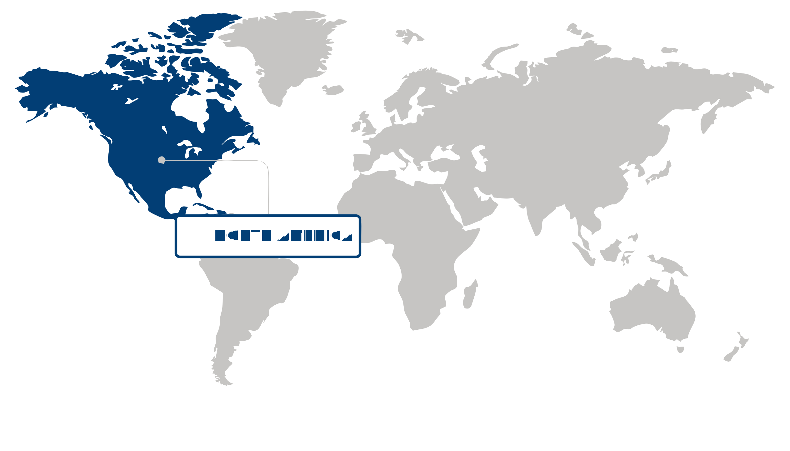
North America (Largest Region)
North America accounted for 37.8% share in 2026, supported by advanced semiconductor manufacturing capabilities, established electronics production infrastructure, and strong adoption of sophisticated packaging and device fabrication technologies. The region benefits from continued investment in semiconductor research, advanced packaging, and high-precision manufacturing processes, where laser debonding equipment is increasingly important for efficient substrate separation and delicate component handling. Growing demand for miniaturized electronic devices and advanced semiconductor architectures is also encouraging manufacturers to adopt automated and highly controlled debonding solutions that improve process consistency and reduce material damage.
Asia Pacific (Fastest-Growing Region)
Asia Pacific is emerging as the fastest-growing region, propelled by expanding semiconductor manufacturing capacity, increasing electronics production, and continued investments in advanced packaging facilities. The region's growing role in the global electronics supply chain is supporting demand for specialized equipment used across wafer processing, packaging, and device manufacturing applications. Rising investments in fabrication facilities and technology upgrades are further encouraging the deployment of precision laser systems, while increasing adoption of smaller and more complex electronic components is creating opportunities for advanced debonding technologies.
| Parameter | North America | Asia Pacific | Europe | Latin America | MEA |
|---|---|---|---|---|---|
| Innovation HubiScaleNascentDeveloping Advanced | |||||
| Cost-Sensitive RegioniScaleLowMedium High | |||||
| Regulatory EnvironmentiScaleRestrictiveNeutral Supportive | |||||
| Demand DriversiScaleWeakModerate Strong | |||||
| Development StageiScaleEmergingDeveloping Developed | |||||
| Adoption RateiScaleLowMedium High | |||||
| New Entrants / StartupsiScaleSparseModerate Dense | |||||
| Macro IndicatorsiScaleWeakStable Strong |
Key Country Insights
United States 🇺🇸
Advanced Packaging AdoptionThe U.S. laser debonding equipment market is closely connected to advanced semiconductor packaging, wafer processing, and heterogeneous integration. Equipment priorities include precise energy control, high process repeatability, automation compatibility, and integration with manufacturing lines handling increasingly sensitive thin-device structures.
Germany 🇩🇪
Precision Equipment EngineeringGermany’s laser debonding equipment market reflects strong demand for precision manufacturing systems used in semiconductor and advanced electronics production. Buyers are likely to prioritize beam-control accuracy, equipment reliability, process monitoring, and seamless integration with automated wafer-handling environments.
Japan 🇯🇵
Wafer Process PrecisionJapan’s laser debonding equipment market is driven by demanding wafer-level and advanced packaging processes where substrate integrity and controlled separation are critical. Equipment suppliers are positioned to emphasize fine process control, low thermal impact, high repeatability, and compatibility with established semiconductor fabrication workflows.
South Korea 🇰🇷
Memory Packaging IntegrationSouth Korea’s laser debonding equipment demand is linked to sophisticated semiconductor manufacturing and packaging processes requiring controlled temporary-bond removal. Commercial priorities include high-throughput automation, precise laser processing, defect reduction, and compatibility with advanced wafer and packaging production platforms.
France 🇫🇷
Specialized Semiconductor ProcessingFrance’s laser debonding equipment market serves specialized semiconductor, photonics, and advanced electronics manufacturing requirements. Buyers are likely to value flexible process configurations, precise laser control, equipment integration, and localized technical support for applications involving delicate substrates and complex device structures.
Italy 🇮🇹
Flexible Process EquipmentItaly’s laser debonding equipment market is positioned around specialized electronics and precision-manufacturing applications where adaptable processing systems can address varied production requirements. Equipment providers can differentiate through configurable laser platforms, process monitoring, automation readiness, and service support for specialized manufacturing environments.
Laser Debonding Equipment Market Share (%), by Technology, 2026
Go beyond the chart, access full insights & data tables
Request Free Sample ReportTechnology Segment Analysis: Laser Ablation (Largest & Fastest-Growing Segment)
The laser ablation segment accounted for the largest 2026 market share of 48.55% of the laser debonding equipment market and is also expected to register the fastest growth, driven by its ability to selectively remove or weaken bonding layers with controlled energy delivery and limited mechanical stress on sensitive substrates. The technology is particularly relevant to advanced semiconductor manufacturing, where temporary bonding materials are used to support thin wafers during processing and must be removed without compromising device integrity. Laser ablation enables localized energy application, supporting precise debonding while reducing the risk of wafer cracking, warpage, and contamination associated with some mechanical or chemical separation methods. Its suitability for demanding manufacturing environments strengthens its appeal as device architectures become more complex and wafer thicknesses decrease. Equipment providers continue to focus on improving beam control, process uniformity, throughput, and compatibility with different bonding materials and substrate configurations. Adoption nevertheless depends on the optical properties of the materials involved, process-window control, equipment integration, and the ability to avoid thermal damage to underlying structures. As semiconductor manufacturers pursue advanced packaging and more efficient wafer-processing workflows, demand for reliable laser ablation-based debonding solutions is expected to expand.
Laser Type Segment Analysis: Ultraviolet (UV) Laser (Largest & Fastest-Growing Segment)
The ultraviolet (UV) laser segment accounted for the largest 42.66% share of the laser debonding equipment market in 2026 and is also expected to grow at the fastest rate, supported by its precision and suitability for processing delicate materials used in semiconductor and advanced electronics manufacturing. UV lasers operate at shorter wavelengths than visible and infrared alternatives, enabling fine energy delivery and effective interaction with selected bonding layers and materials. These characteristics can facilitate controlled debonding with limited heat diffusion into adjacent structures, an important consideration when handling thin wafers and temperature-sensitive components. UV-based systems are therefore well suited to applications requiring high positional accuracy, clean separation, and consistent process outcomes. Their continued adoption is supported by the increasing complexity of semiconductor packaging and the need to protect fragile substrates during manufacturing. Performance, however, depends on material absorption characteristics, pulse parameters, optical-system design, and process optimization. Equipment cost, maintenance requirements, and integration with existing production lines can also influence purchasing decisions. Continued improvements in laser stability, beam delivery, and process monitoring are expected to strengthen the role of UV lasers in precision debonding applications.
Application Segment Analysis: Semiconductor Wafer Debonding (Largest & Fastest-Growing Segment)
The semiconductor wafer debonding segment accounted for the largest market share of 55.93% in 2026 within the laser debonding equipment market and is also expected to register the fastest growth, reflecting the growing importance of temporary wafer bonding and controlled substrate separation in advanced semiconductor manufacturing. Wafer debonding is essential in processes where thin or fragile wafers require mechanical support during grinding, thinning, lithography, or packaging operations before being separated from temporary carriers. Laser-based methods offer localized energy delivery that can facilitate separation while reducing mechanical loading on delicate wafers and minimizing the risk of breakage or surface damage. These capabilities are increasingly relevant as manufacturers develop advanced packaging architectures, including heterogeneous integration and other approaches that require precise handling of thin substrates. Demand is further influenced by requirements for higher process yields, consistent separation quality, and compatibility with diverse bonding materials. Successful implementation depends on the interaction between laser parameters, adhesive properties, wafer materials, and process conditions, making process development and equipment calibration critical. As semiconductor fabrication and packaging workflows become more demanding, manufacturers are likely to place greater emphasis on debonding systems that combine precision, throughput, and repeatability while protecting wafer integrity.
| Segment | Sub-Segment | Largest Segment | Fastest Growing |
|---|---|---|---|
| Technology | Laser-Induced Breakdown Spectroscopy (LIBS), Laser Ablation, Laser-Induced Forward Transfer (LIFT) | Laser Ablation | Laser Ablation |
| Laser Type | Ultraviolet (UV) Laser, Infrared (IR) Laser, Pulsed Laser, Others | Ultraviolet (UV) Laser | Ultraviolet (UV) Laser |
| Application | Semiconductor Wafer Debonding, Solar Cell Interconnect Debonding, Medical Device Debonding, Others | Semiconductor Wafer Debonding | Semiconductor Wafer Debonding |
Unlock insights tailored to your business with our bespoke market research solutions.
Click to get your customized report now.
Competitive Landscape and Market Positioning
Analyst Perspective:
In advanced semiconductor packaging, laser debonding equipment providers compete primarily on process safety, precision, and throughput integration. Achieving optimal wavelength control is critical to ensure clean release layer interaction without inducing thermal stress or physical damage to delicate, high-value substrates. However, raw laser power and fast cycle times yield commercial value only when paired with steady yield, high uptime, and flexible handling across varied wafer geometries. Equipment vendors must prove broad compatibility across diverse material stacks and temporary carriers while maintaining tight process windows. Ultimately, seamless factory integration—spanning automated handling, thermal mitigation, and reliable post-release cleanliness—dictates adoption in modern electronics manufacturing.
Major players in the laser debonding equipment market:
- EV Group (Austria)
- SUSS MicroTec (Germany)
- ASMPT (Singapore)
- DISCO Corporation (Japan)
- Tokyo Electron (Japan)
- KLA (US)
- Nikon (Japan)
- Canon (Japan)
- Applied Materials (US)
- Hanmi Semiconductor (South Korea)
| Company | Market Share | Company Revenue | Revenue CAGR (%) | Product Portfolio | Geographic Presence | Innovation / R&D Focus | Strategic Developments |
|---|---|---|---|---|---|---|---|
| EV Group (Austria) | |||||||
| SUSS MicroTec (Germany) | |||||||
| ASMPT (Singapore) | |||||||
| DISCO Corporation (Japan) | |||||||
| Tokyo Electron (Japan) | |||||||
| KLA (US) | |||||||
| Nikon (Japan) | |||||||
| Canon (Japan) | |||||||
| Applied Materials (US) | |||||||
| Hanmi Semiconductor (South Korea) |
Industry Development/News
| Company Name | Date | Key Development |
|---|---|---|
| EV Group | June 2024 | EV Group entered into a strategic partnership with Fraunhofer IZM-ASSID to develop and optimize alternative bonding and debonding technologies. The collaboration targets advanced CMOS and heterogeneous integration applications, including quantum computing, leveraging joint research capabilities in 3D wafer-level system integration. |
| EV Group | May 2024 | EV Group advanced its semiconductor layer transfer technology by doubling production throughput using its proprietary LayerRelease system. The infrared laser and inorganic release material approach achieves nanometer-level precision on silicon carriers, removing the need for glass substrates and organic adhesives in advanced packaging workflows. |
Customize Your Report
Explore examples of how this report can be tailored to different research needs, including custom segments, additional topics or chapters, and related reports. Click a section of the wheel or its numbered marker to explore the available options.
Laser Debonding Equipment Market — Custom Segments
| Segment | Sub-Segment |
|---|---|
| Wafer Size Compatibility | Up to 200 mm, 300 mm, Above 300 mm |
| Automation Level | Manual, Semi-Automated, Fully Automated |
| Equipment Configuration | Standalone Systems, Integrated Production-Line Systems, Cluster / Multi-Module Systems |
Laser Debonding Equipment Market — Custom TOC
| Custom Chapter | Chapter Details |
|---|---|
| Semiconductor Packaging Transition Impact |
|
| Equipment Lifecycle Economics |
|
| Process Integration Strategies |
|
Need a different cut of the data?
Request Custom ResearchFrequently Asked Questions
What is the estimated worth of the laser debonding equipment market?
What is the anticipated CAGR of the laser debonding equipment industry?
How is the shift toward minimally invasive orthodontic care influencing laser debonding equipment adoption?
How are equipment technology advancements supporting broader clinical adoption of laser debonding?
Why does laser ablation lead the laser debonding equipment market?
How are semiconductor wafer debonding applications driving market growth?
What makes North America the leading market for laser debonding equipment?
How is Asia Pacific accelerating demand for laser debonding equipment?
Which companies dominate the laser debonding equipment landscape?
Our Clients
"Working with FBI has been a good experience. The market report provided a holistic view, covering everything from emerging trends to potential risks."
Semtech Corporation
"The experience was highly positive. The team showcased remarkable flexibility in adapting to our specific needs and delivered report that perfectly aligned with all our requirements."
TSMC
"What really stood out to me was how clearly and promptly the Fundamental Business Insights team communicated throughout. It made the collaboration feel effortless."
NXP Semiconductors
Our Research Team & Methodology
Every Fundamental Business Insights report is built by a dedicated vertical research team, validated through a structured primary-and-secondary methodology, and reviewed for accuracy before it reaches you.
This report was prepared by the Electronics & Semiconductors Research Team at Fundamental Business Insights, a dedicated research group specializing in the global electronics and semiconductor ecosystem. Our analysts continuously monitor technology innovations, manufacturing trends, competitive developments, supply chain dynamics, regulatory changes, and end-user demand to deliver timely market intelligence. The research is developed using a structured methodology that combines primary industry interactions, company financial disclosures, government publications, trade associations, technical literature, patent analysis, and other authoritative secondary sources. Market estimates are validated through multiple research techniques, including top-down and bottom-up analysis, before undergoing an internal quality review to ensure accuracy, consistency, and methodological integrity prior to publication.
Delivery
Published
Available
Support
- Market Size & Forecast
- Market Segmentation
- Regional Analysis
- Growth Drivers & Challenges
- Market Dynamics
- Competitive Landscape
- Company Profiles
- Competitive Benchmarking
- Mergers & Acquisitions
- Market Share Analysis or Key Company Strategies
- Value Chain Analysis
- Porter's Five Forces
- PESTLE Analysis
- Pricing Trends
- Supply-Demand Analysis
- Technology Landscape
- Regulatory Landscape
- Investment & Funding Landscape
- Emerging Opportunities
- Future Market Outlook