Photonic Crystals for Optical Computing Market Size & Growth Forecast 2027–2036, By Segments (Computing Function, Integration Type, Material Platform, Product Type, End Use Industry), Regional Demand Trends (North America, Asia Pacific, Europe), Key Country Insights (U.S., Japan, South Korea, Germany, France, Italy), and Competitive Landscape
Jump to Content
Market Size and Growth Outlook
Photonic Crystals for Optical Computing Market size was around USD 4.85 billion in 2026 and is slated to grow at a 21.22% CAGR from 2027 to 2036, attaining USD 33.23 billion by 2036. The industry revenue for 2027 is assessed at USD 5.76 billion.
Get more details on this report
Request Free Sample ReportPhotonic Crystals for Optical Computing Market Intelligence Snapshot
Regional Market Dynamics
- Europe accounted for 37.04% of the market in 2026, supported by advanced photonics infrastructure, strong research capabilities, and collaboration between academic institutions and technology developers.
- Asia Pacific is expected to grow fastest as semiconductor manufacturing, photonics research, AI applications, and high-performance computing investments increase demand for energy-efficient optical computing technologies.
Segment Momentum
- Digital optical computing held a 42.98% market share in 2026, supported by photonic crystals' ability to control light propagation and enable parallel processing, low-latency signal handling, and compact optical computing architectures.
- Phase-change materials are the fastest-growing material platform, driven by their reconfigurable optical properties. They enable programmable switching, optical memory, adaptive signal processing, and reconfigurable photonic circuits for advanced computing architectures.
Market Expansion Drivers
- Rising demand for ultra-high-speed and low-energy optical computing architectures.
- Advancements in nanofabrication enabling scalable photonic crystal devices.
- Government and defense funding for next-generation computing research.
Leading Market Participants
- Major players in the photonic crystals for optical computing market include Intel (US), IBM (US), NTT (Japan), Fujitsu (Japan), Hamamatsu Photonics (Japan), Hewlett Packard Enterprise (US), Nokia Bell Labs (US), Huawei (China), STMicroelectronics (Switzerland), imec (Belgium).
Global Market Forecast Snapshot
Market Outlook
- 2026 Market Size: USD 4.85 billion
- 2027 Estimated Market Size: USD 5.76 billion
- Projected Market Size: USD 33.23 billion by 2036
- Growth Forecast: 21.22% CAGR (2027-2036)
Regional and Segment Outlook
- Leading Regional Market: Europe
- High-Growth Regional Hub: Asia Pacific
- Core Revenue Segment: Computing Function (Digital Optical Computing) | Integration Type (Monolithic Integration) | Material Platform (Silicon-on-insulator (SOI)) | Product Type (2D Photonic Crystals) | End Use Industry (Data Centers & Cloud Computing)
- Emerging Opportunity Segment: Computing Function (Neuromorphic Optical Computing) | Integration Type (Hybrid Integration) | Material Platform (Phase-change Materials) | Product Type (3D Photonic Crystals) | End Use Industry (High-performance Computing)
Market Growth Drivers and Industry Trends
Rising demand for ultra-high-speed and low-energy optical computing architectures
The growing need for computing architectures capable of handling intensive workloads with greater speed and energy efficiency is accelerating interest in photonic approaches to information processing. Photonic crystals can manipulate and control light at extremely small scales, enabling the development of optical components that support rapid signal transmission and processing while reducing reliance on conventional electronic pathways. Their ability to facilitate compact and highly controllable optical functions makes them attractive for applications involving artificial intelligence, high-performance computing, telecommunications, and data-intensive processing. As conventional computing architectures face increasing challenges related to energy consumption, heat generation, and data movement, photonic crystal-based technologies are gaining attention as potential building blocks for next-generation computing systems.
Advancements in nanofabrication enabling scalable photonic crystal devices
Progress in nanofabrication techniques is improving the ability to design and manufacture photonic crystal structures with greater precision, consistency, and functional complexity. Advanced lithography, material processing, and nanoscale patterning methods are enabling tighter control over the geometry and optical properties of photonic structures, supporting the development of increasingly sophisticated devices. Improvements in fabrication processes are also helping address challenges related to miniaturization, manufacturing repeatability, and integration with other photonic and electronic components. As fabrication capabilities become more compatible with scalable production approaches, the expanding feasibility of compact photonic devices is expected to support wider adoption across optical computing and related applications.
Government and defense funding for next-generation computing research
Government and defense support for advanced computing research is contributing to the development of photonic technologies by providing resources for research programs focused on high-performance, secure, and energy-efficient computing architectures. Funding in this area can support fundamental research, prototype development, advanced materials investigation, and the transition of laboratory concepts toward practical systems. Photonic crystal technologies benefit from such initiatives because their development often requires multidisciplinary expertise spanning optics, materials science, nanotechnology, and computer engineering. Continued institutional support for next-generation computing capabilities is therefore helping accelerate technological maturity and expand the research ecosystem surrounding optical processing solutions.
| Growth Driver | Impact on CAGR | Regulatory Influence | Geographic Relevance | Adoption Rate | Impact Timeline |
|---|---|---|---|---|---|
| Rising demand for ultra-high-speed and low-energy optical computing architectures | 4.2% | Medium term (2–5 yrs) | North America; Europe; Asia Pacific | Medium | Moderate |
| Advancements in nanofabrication enabling scalable photonic crystal devices | 3.6% | Long term (5+ yrs) | Asia Pacific; North America | Low | Slow |
| Government and defense funding for next-generation computing research | 3.1% | Short term (≤ 2 yrs) | North America; Europe | High | Moderate |
Explore Growth Opportunities
Request Free Sample ReportRegional Demand Dynamics
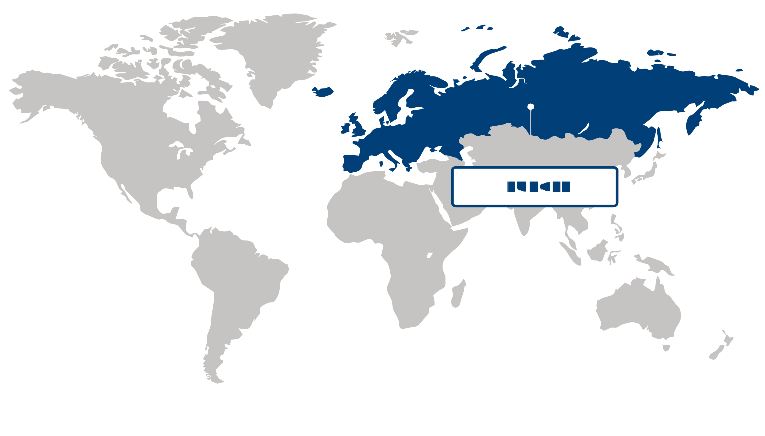
Europe (Largest Region)
The photonic crystals for optical computing market in Europe held the largest share in 2026, accounting for 37.04% of the market, impelled by strong research capabilities, advanced photonics infrastructure, and growing investments in next-generation computing technologies. European research institutions and technology developers are actively advancing photonic components that can improve computing efficiency, data processing, and high-speed information transmission. Increasing demand for energy-efficient computing architectures is also encouraging the development of optical computing solutions that can address limitations associated with conventional electronic systems. In addition, strong collaboration between academic institutions, research organizations, and industrial technology developers is supporting innovation in photonic crystal design and optical computing applications, creating a favorable environment for market development.
Asia Pacific (Fastest-Growing Region)
The photonic crystals for optical computing market in Asia Pacific is expected to experience the fastest growth, supported by expanding semiconductor and electronics industries, increasing investments in photonics research, and rising demand for high-performance computing technologies. Countries across the region are strengthening capabilities in advanced semiconductor manufacturing, optical communications, and emerging computing architectures, creating opportunities for photonic crystal-based components. The growing use of artificial intelligence, data-intensive applications, and high-speed communication systems is further increasing the need for computing technologies capable of delivering improved processing performance and energy efficiency. Moreover, government support for advanced technology development and increasing investments in research and development are encouraging innovation in integrated photonics and optical computing, supporting rapid regional market expansion.
| Parameter | North America | Asia Pacific | Europe | Latin America | MEA |
|---|---|---|---|---|---|
| Innovation HubiScaleNascentDeveloping Advanced | |||||
| Cost-Sensitive RegioniScaleLowMedium High | |||||
| Regulatory EnvironmentiScaleRestrictiveNeutral Supportive | |||||
| Demand DriversiScaleWeakModerate Strong | |||||
| Development StageiScaleEmergingDeveloping Developed | |||||
| Adoption RateiScaleLowMedium High | |||||
| New Entrants / StartupsiScaleSparseModerate Dense | |||||
| Macro IndicatorsiScaleWeakStable Strong |
Key Country Insights
United States 🇺🇸
Advanced Computing IntegrationThe U.S. market is prioritizing photonic crystal technologies that can integrate with AI accelerators, optical interconnects, and high-performance computing architectures. Near-term commercial activity is likely to center on improving fabrication scalability, coupling efficiency, and compatibility with existing semiconductor manufacturing ecosystems.
Germany 🇩🇪
Precision Photonics EngineeringGermany is emphasizing photonic crystal development for precision optical processing, industrial computing, and advanced manufacturing applications. Market priorities include improving device reliability, fabrication precision, and integration with established photonics and semiconductor equipment capabilities to support deployment beyond laboratory-scale optical computing systems.
Japan 🇯🇵
Integrated Photonics DevelopmentJapan is focusing on compact photonic crystal architectures suited to optical signal processing, communications, and next-generation computing components. Japan’s market priorities include miniaturization, high-efficiency optical devices, and integration with sophisticated electronics manufacturing processes, supporting commercialization of photonic computing components in specialized applications.
South Korea 🇰🇷
Semiconductor Photonics IntegrationSouth Korea is positioning photonic crystal technologies around their integration with advanced semiconductor and data-processing hardware. Commercial priorities center on manufacturable photonic structures, high-speed optical interconnects, and compatibility with semiconductor packaging, particularly where optical computing can address bandwidth and energy-efficiency requirements.
France 🇫🇷
Research-Led Optical InnovationFrance is advancing photonic crystal applications through strong research and engineering capabilities spanning optical computing and integrated photonics. Market attention is shifting toward translating laboratory designs into manufacturable devices, with priorities including optical switching, nonlinear processing, and integration into scalable photonic platforms.
Italy 🇮🇹
Specialized Photonic ComponentsItaly is concentrating on specialized photonic crystal components for optical processing and integrated photonics applications. Commercial priorities include device customization, precision fabrication, and integration into application-specific optical systems, creating opportunities where photonic computing architectures require tailored components rather than standardized semiconductor solutions.
Photonic Crystals for Optical Computing Market Share (%), by Computing Function, 2026
Go beyond the chart, access full insights & data tables
Request Free Sample ReportComputing Function Segment Analysis: Digital Optical Computing (Largest Segment) vs Neuromorphic Optical Computing (Fastest-Growing Segment)
Digital optical computing accounted for the largest share of 42.98% in 2026 in the computing function segment, reflecting its established role in photonic crystal-based optical computing architectures designed to perform high-speed computational operations through the manipulation of light. Digital optical computing benefits from the ability of photonic structures to control light propagation, enabling parallel processing, low-latency signal handling, and efficient execution of computational tasks. Its adoption is supported by growing interest in optical approaches for applications where conventional electronic systems face limitations related to data movement, processing speed, and energy consumption. Photonic crystals provide precise control over optical modes and signal routing, making them suitable for developing compact computing architectures that can support advanced data-processing workloads. Continued progress in photonic device fabrication, optical interconnects, and integrated computing architectures is reinforcing the role of digital optical computing as a foundational application in the market.
Neuromorphic optical computing is expected to register the fastest growth in the computing function segment, driven by increasing interest in computing architectures that emulate neural processing through optical signals and photonic structures. Photonic crystals can support the development of compact optical components capable of controlling and transforming light in ways relevant to neural-network operations, pattern recognition, and parallel information processing. The segment is gaining momentum as demand increases for computing approaches that can process complex workloads with high parallelism and reduced data-transfer bottlenecks. The integration of optical signal processing with neuromorphic principles also creates opportunities for efficient artificial intelligence and machine-learning architectures, particularly where rapid inference and energy-efficient computation are important. Advances in programmable photonics, optical nonlinearities, and integrated photonic platforms are expected to further support the development of neuromorphic optical computing applications.
Integration Type Segment Analysis: Monolithic Integration (Largest Segment) vs Hybrid Integration (Fastest-Growing Segment)
Monolithic integration represented the largest segment in 2026 in the integration type category, reflecting the importance of integrating photonic crystal structures and associated optical components onto a common platform. Monolithic integration can provide compact device architectures, improved component alignment, and reduced interconnection complexity, making it attractive for optical computing systems where size, performance, and integration efficiency are important. Integrating multiple photonic functions on a single platform can also improve signal routing and reduce losses associated with external connections. The approach is particularly relevant to the development of scalable optical computing architectures, where dense integration of optical components is needed to support increasingly complex computational functions. Ongoing improvements in semiconductor and photonic fabrication processes are strengthening the feasibility of monolithic architectures for advanced optical computing applications.
Hybrid integration is expected to experience the fastest growth in the integration type segment as developers seek to integrate different material systems and device technologies to optimize optical computing performance. Hybrid optical architectures can bring together complementary capabilities from distinct photonic, electronic, and material platforms, enabling greater flexibility in designing high-performance systems. This approach is particularly useful where a single material platform cannot simultaneously provide all the required optical, electrical, switching, and computational characteristics. The growing complexity of optical computing architectures is increasing demand for integration methods that allow specialized components to operate together in a unified system. Advances in heterogeneous photonics, packaging technologies, and optical interconnect design are expected to further accelerate the adoption of hybrid integration for next-generation photonic computing platforms.
Material Platform Segment Analysis: Silicon-on-insulator (SOI) (Largest Segment) vs Phase-change Materials (Fastest-Growing Segment)
Silicon-on-insulator (SOI) accounted for the largest position in the material platform segment in 2026, supported by its established compatibility with integrated photonics manufacturing and its suitability for developing compact photonic crystal structures. SOI platforms provide strong optical confinement and enable the integration of multiple photonic components in a relatively compact architecture, making them well suited to optical computing applications. Their compatibility with established semiconductor fabrication techniques also supports repeatable device production and integration with electronic components. SOI-based photonic structures can facilitate efficient control of light propagation, optical routing, modulation, and signal processing, which are central requirements for photonic computing systems. Continued development of silicon photonics and integrated optical architectures is expected to sustain the importance of SOI as a core material platform for photonic crystal-based computing.
Phase-change materials are projected to be the fastest-growing material platform, driven by their ability to provide dynamically reconfigurable optical properties that are valuable for advanced computing architectures. These materials can change their optical characteristics in response to controlled stimuli, creating opportunities for programmable switching, optical memory, adaptive signal processing, and reconfigurable photonic circuits. Their integration with photonic crystals can enable optical devices whose behavior can be modified after fabrication, supporting computing systems that require flexibility and dynamic functionality. Increasing interest in programmable photonics, in-memory computing, and neuromorphic architectures is creating additional opportunities for phase-change material platforms. As fabrication and integration techniques continue to improve, phase-change materials are expected to gain broader relevance in advanced photonic computing systems where reconfigurability and multifunctional optical processing are key requirements.
| Segment | Sub-Segment | Largest Segment | Fastest Growing |
|---|---|---|---|
| Computing Function | Digital Optical Computing, Analog Optical Computing, Quantum Optical Computing, Neuromorphic Optical Computing | Digital Optical Computing | Neuromorphic Optical Computing |
| Integration Type | Monolithic Integration, Hybrid Integration, Total Consumption | Monolithic Integration | Hybrid Integration |
| Material Platform | Silicon-on-insulator (SOI), III-V Semiconductors, Phase-change Materials | Silicon-on-insulator (SOI) | Phase-change Materials |
| Product Type | 1D Photonic Crystals, 2D Photonic Crystals, 3D Photonic Crystals | 2D Photonic Crystals | 3D Photonic Crystals |
| End Use Industry | Data Centers & Cloud Computing, Telecommunications, Defense & Aerospace, Research Institutions, High-performance Computing | Data Centers & Cloud Computing | High-performance Computing |
Unlock insights tailored to your business with our bespoke market research solutions.
Click to get your customized report now.
Competitive Landscape and Market Positioning
Analyst Perspective:
Competitive positioning in the photonic crystals for optical computing market depends on translating precise optical control into scalable, integrated computing components. Accurate bandgap engineering and efficient light confinement are essential for predictable device behavior, while minimizing insertion loss and maintaining efficient signal routing influence performance at the system level. Integration with silicon photonic circuits offers a pathway toward compact architectures, although compatibility across geometries, fabrication processes, and optical interfaces remains important. Manufacturing scalability presents a further challenge, as sub-micron dimensional variations can affect optical specifications, consistency, and production yield. Consequently, the strongest commercial prospects rest on combining reliable optical performance with integration efficiency and repeatable manufacturing, rather than optimizing individual device characteristics in isolation.
Prominent players in the photonic crystals for optical computing market:
- Intel (US)
- IBM (US)
- NTT (Japan)
- Fujitsu (Japan)
- Hamamatsu Photonics (Japan)
- Hewlett Packard Enterprise (US)
- Nokia Bell Labs (US)
- Huawei (China)
- STMicroelectronics (Switzerland)
- imec (Belgium)
| Company | Market Share | Company Revenue | Revenue CAGR (%) | Product Portfolio | Geographic Presence | Innovation / R&D Focus | Strategic Developments |
|---|---|---|---|---|---|---|---|
| Intel (US) | |||||||
| IBM (US) | |||||||
| NTT (Japan) | |||||||
| Fujitsu (Japan) | |||||||
| Hamamatsu Photonics (Japan) | |||||||
| Hewlett Packard Enterprise (US) | |||||||
| Nokia Bell Labs (US) | |||||||
| Huawei (China) | |||||||
| STMicroelectronics (Switzerland) | |||||||
| imec (Belgium) |
Industry Development/News
| Company Name | Date | Key Development |
|---|---|---|
| Shanghai Jiao Tong University and Sun Yat-Sen University | September 2025 | Researchers developed a breakthrough method to generate pseudomagnetic fields in silicon photonic crystals by varying local unit symmetry. The technique enables spatial control of light flow and demonstrates compact S-shaped waveguide bends transmitting 140 Gbps data using PAM-4 modulation. |
| Q.ANT | April 2025 | Q.ANT unveiled its photonic Native Processing Server utilizing proprietary thin-film lithium niobate photonic chips to execute complex nonlinear mathematical operations in the optical domain. The commercial architecture delivers significant improvements in energy efficiency and compute density while integrating via standard PCI Express interfaces. |
Customize Your Report
Explore examples of how this report can be tailored to different research needs, including custom segments, additional topics or chapters, and related reports. Click a section of the wheel or its numbered marker to explore the available options.
Photonic Crystals for Optical Computing Market — Custom Segments
| Segment | Sub-Segment |
|---|---|
| Optical Performance Tier | Standard-performance photonic crystals, High-performance photonic crystals, Ultra-high-performance photonic crystals |
| Buyer Type | Computing & data center operators, Telecommunications companies, Defense & aerospace organizations, Research institutions, Semiconductor & photonics companies |
| Commercialization Stage | Research-stage systems, Prototype systems, Pilot deployments, Commercial deployments |
Photonic Crystals for Optical Computing Market — Custom TOC
| Custom Chapter | Chapter Details |
|---|---|
| Commercialization Readiness Assessment |
|
| Fabrication Ecosystem & Supply Constraints |
|
| Application Adoption Pathways |
|
Need a different cut of the data?
Request Custom ResearchFrequently Asked Questions
What is the market valuation of the photonic crystals for optical computing market?
What is the projected value of the photonic crystals for optical computing industry by 2036?
How is demand for high-speed, energy-efficient computing accelerating photonic crystal adoption?
How are nanofabrication advances improving the commercial potential of photonic crystal devices?
Why does digital optical computing lead the photonic crystals for optical computing market?
How are phase-change materials creating growth opportunities in photonic crystal-based optical computing?
Why does Europe lead the photonic crystals for optical computing market?
How is Asia Pacific driving growth in the photonic crystals for optical computing market?
Which organizations are considered leaders in the photonic crystals for optical computing landscape?
Our Clients
"Working with FBI has been a good experience. The market report provided a holistic view, covering everything from emerging trends to potential risks."
Semtech Corporation
"The experience was highly positive. The team showcased remarkable flexibility in adapting to our specific needs and delivered report that perfectly aligned with all our requirements."
TSMC
"What really stood out to me was how clearly and promptly the Fundamental Business Insights team communicated throughout. It made the collaboration feel effortless."
NXP Semiconductors
Our Research Team & Methodology
Every Fundamental Business Insights report is built by a dedicated vertical research team, validated through a structured primary-and-secondary methodology, and reviewed for accuracy before it reaches you.
This report was prepared by the Electronics & Semiconductors Research Team at Fundamental Business Insights, a dedicated research group specializing in the global electronics and semiconductor ecosystem. Our analysts continuously monitor technology innovations, manufacturing trends, competitive developments, supply chain dynamics, regulatory changes, and end-user demand to deliver timely market intelligence. The research is developed using a structured methodology that combines primary industry interactions, company financial disclosures, government publications, trade associations, technical literature, patent analysis, and other authoritative secondary sources. Market estimates are validated through multiple research techniques, including top-down and bottom-up analysis, before undergoing an internal quality review to ensure accuracy, consistency, and methodological integrity prior to publication.
Delivery
Published
Available
Support
- Market Size & Forecast
- Market Segmentation
- Regional Analysis
- Growth Drivers & Challenges
- Market Dynamics
- Competitive Landscape
- Company Profiles
- Competitive Benchmarking
- Mergers & Acquisitions
- Market Share Analysis or Key Company Strategies
- Value Chain Analysis
- Porter's Five Forces
- PESTLE Analysis
- Pricing Trends
- Supply-Demand Analysis
- Technology Landscape
- Regulatory Landscape
- Investment & Funding Landscape
- Emerging Opportunities
- Future Market Outlook