Plasma Etching Equipment Market Size & Forecasts 2026-2035, By Segments (Type, Technology, Application, Industry Vertical), Growth Opportunities, Innovation Landscape, Regulatory Shifts, Strategic Regional Insights (U.S., Japan, China, South Korea, UK, Germany, France), and Competitive Dynamics (Lam Research, Applied Materials, Tokyo Electron, Hitachi High-Tech, SCREEN Semiconductor Solutions)
Market Size and Growth Outlook
Plasma Etching Equipment Market size is estimated to increase from USD 12.65 billion in 2025 to USD 26.32 billion by 2035, supported by a CAGR exceeding 7.6% during 2026-2035. In 2026, revenues are forecast to reach USD 13.49 billion.
Get more details on this report
Request Free Sample ReportPlasma Etching Equipment Market Intelligence Snapshot
Regional Market Dynamics
Segment Momentum
Market Expansion Drivers
Leading Market Participants
Global Market Forecast Snapshot
Market Outlook
Regional and Segment Outlook
Market Growth Drivers and Industry Trends
The increasing complexity of semiconductor manufacturing, driven by the transition to advanced nodes such as 5nm and below, is a critical growth driver for the plasma etching equipment market. As highlighted in semiconductor-focused press releases from Intel and TSMC, plasma etching enables precise patterning essential for scaling down transistor sizes while maintaining performance and power efficiency. This shift is propelled by heightened consumer demand for high-performance electronics and data-intensive applications, necessitating innovation in lithography and etching processes. For established manufacturers and new entrants, this creates an opportunity to develop highly specialized, next-generation etchers with enhanced accuracy and selectivity. The ongoing capacity expansions and technology refinements at leading foundries suggest sustained demand for plasma etching systems closely aligned with industry node progression strategies.
Growth of 3D Structures Like 3D NAND and FinFET Architectures
The evolution toward three-dimensional semiconductor architectures such as 3D NAND and FinFET transistors is fueling the plasma etching equipment market by requiring novel etching solutions capable of handling complex vertical geometries. According to a roadmap published by the Semiconductor Equipment and Materials International (SEMI) association, achieving high aspect ratio etching with uniformity and minimal damage is paramount for these structures. This technological pivot reflects a broader industry focus on improving chip density and energy efficiency, responding to the surge in data storage and mobile device proliferation. Equipment makers can capitalize on this trend by advancing their plasma etching platforms to offer deeper etching capabilities and enhanced process control. Market leaders investing in R&D for 3D structure compatibility will differentiate themselves, while startups can target niche applications within this expanding technical landscape.
Long-Term Shift to New Substrate Materials Enhancing Etching Needs
The transition from traditional silicon to alternative substrates—such as silicon carbide (SiC) and gallium nitride (GaN)—is reshaping the plasma etching equipment market by introducing new material-specific processing challenges. Government agencies like the U.S. Department of Energy emphasize SiC and GaN’s critical role in power electronics and electric vehicle technologies due to their superior electrical and thermal properties. These materials require tailored etching chemistries and equipment capable of managing different etch rates and surface characteristics. This shift opens strategic opportunities for equipment vendors to innovate plasma etching solutions customized for emerging substrate materials, addressing a growing segment of the chip manufacturing ecosystem. As these materials gain adoption across automotive and industrial sectors, demand for adapted plasma etching technologies is expected to remain robust in line with evolving substrate preferences.
Industry Restraints:
High Capital Expenditure Requirements
The plasma etching equipment market is significantly restrained by its intensive capital expenditure demands, as the acquisition and maintenance of advanced etching systems involves substantial upfront investment. This financial barrier slows adoption across semiconductor manufacturers, particularly among SMEs and emerging players lacking robust capital reserves. Lam Research Corporation’s 2023 financial disclosures illustrate that capital costs for next-generation etchers have escalated due to sophisticated process controls and precision components. The high cost limits rapid scaling, complicating entry for startups and restricting expansion for incumbents operating under cost containment pressures. Strategically, firms must balance R&D investments against capital availability, prolonging decision cycles and delaying launch of innovative tools. Moving forward, the intense capital outlay will persist as a core constraint, compelling market participants to seek financing solutions or collaborative models to mitigate financial exposure and sustain technology advancement.
Stringent Environmental Regulatory Constraints
Environmental regulations increasingly restrict plasma etching equipment usage, due to the potential release of hazardous chemicals and greenhouse gases. Governments and regulatory bodies like the U.S. Environmental Protection Agency (EPA) have tightened emissions standards, affecting manufacturers’ operational flexibility. For instance, EPA’s updated Maximum Achievable Control Technology (MACT) standards impose rigorous limits on perfluorocarbon emissions, critical to plasma etching processes, raising compliance costs as documented by industry analysis from SEMI. These regulations necessitate costly upgrades or redesigns of equipment to align with stricter environmental protocols, impeding market speed and innovation cycles. Both established players and new entrants face delays and elevated barriers in product certification and market entry. As climate actions intensify globally, regulatory constraints will remain a pivotal challenge, encouraging companies to prioritize sustainable technology development and proactive regulatory strategies to maintain competitiveness.
| Growth Driver | Impact on CAGR | Regulatory Influence | Geographic Relevance | Adoption Rate | Impact Timeline |
|---|---|---|---|---|---|
| Rising use of plasma etching for advanced semiconductor nodes | 1.20% | Short term (≤ 2 yrs) | Asia Pacific (Primary), North America (Spillover) | Low | Fast |
| Growth of 3D structures (3D NAND, FinFET) requiring etching | 1.00% | Medium term (2–5 yrs) | North America (Primary), Europe (Spillover) | Medium | Moderate |
| Long-term shift to new substrate materials enhancing etching needs | 0.80% | Long term (5+ yrs) | Europe (Primary), Asia Pacific (Spillover) | High | Slow |
Unlock insights tailored to your business with our bespoke market research solutions.
Click to get your customized report now.
Regional Demand Dynamics
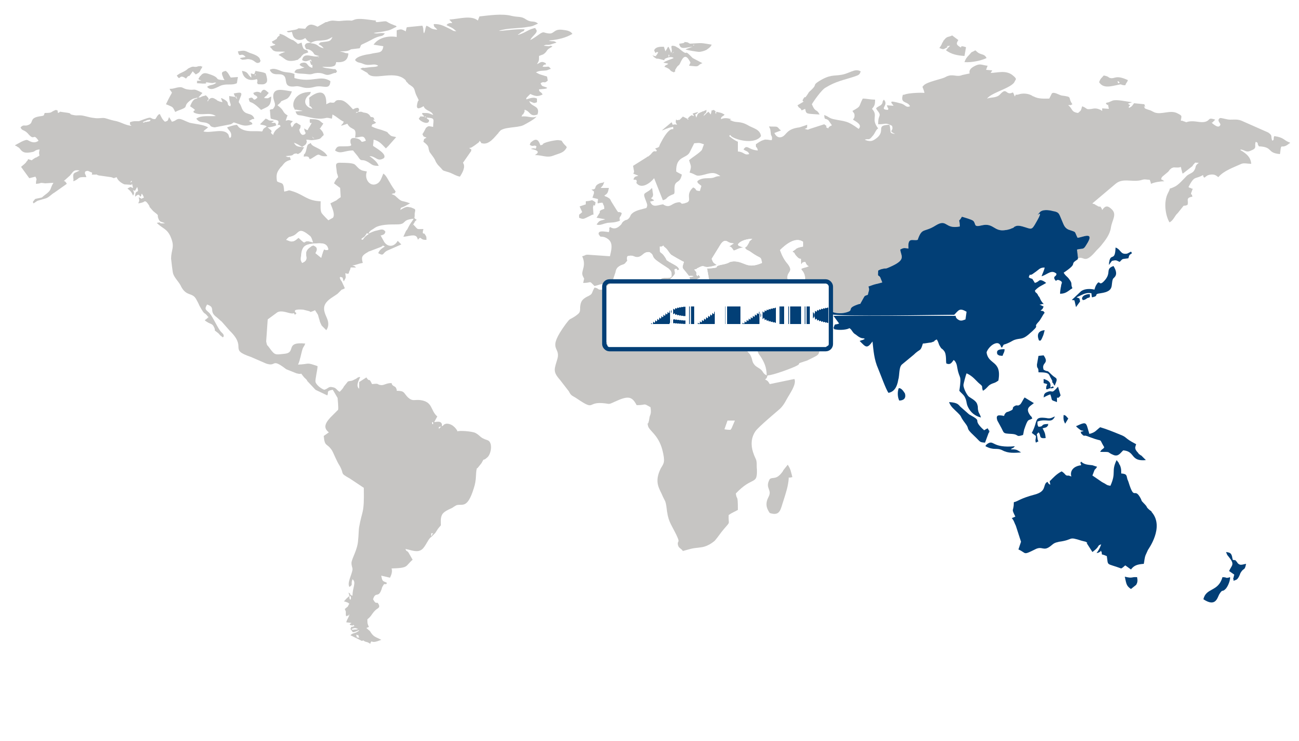
Asia Pacific dominates the plasma etching equipment market, capturing over 41.2% of the global share in 2025 and emerging as the fastest-growing region with an 8.9% CAGR. This leadership stems primarily from the region’s robust presence of advanced node logic and memory fabrication facilities, notably propelling demand for high-precision etching technologies. Major semiconductor hubs such as Taiwan, South Korea, and Singapore bolster operational advancements and supply chain resilience, enabling cutting-edge process innovations. According to a corporate press release by Taiwan Semiconductor Manufacturing Company (TSMC), ongoing investments in 3nm and 2nm nodes are intensifying the requirement for state-of-the-art plasma etching equipment. Policymaking in countries like South Korea also favors high-tech manufacturing, enhancing regional competitiveness. Consequently, Asia Pacific presents compelling opportunities for plasma etching equipment vendors seeking to capitalize on sustained capital expenditures and continuous technological evolution.
Japan is positioned as a pivotal hub in the Asia Pacific plasma etching equipment market, supported by its concentration of leading semiconductor equipment manufacturers and research institutions. Japan’s strategic emphasis on precision manufacturing and quality control drives adoption of innovative plasma etching solutions, as highlighted by Kokusai Electric’s recent product launches emphasizing eco-efficiency and cost-effectiveness. Regulatory frameworks promoting sustainable manufacturing further accelerate deployment of advanced etching technologies. This environment enables Japan to function as both a market for equipment sales and a center for equipment innovation, enhancing Asia Pacific’s regional leadership. Consequently, Japan’s integration of manufacturing excellence with technological innovation underpins broader growth trajectories in the plasma etching equipment market.
China anchors the Asia Pacific plasma etching equipment market through its large-scale semiconductor fabrication expansion and government-driven initiatives such as “Made in China 2025,” which targets self-sufficiency in semiconductor technology. Rapid capacity additions by major fabs like Semiconductor Manufacturing International Corporation (SMIC) are intensifying demand for plasma etching equipment suited to advanced node production. Additionally, China’s evolving regulatory landscape incentivizes sustainable and efficient production methods, driving demand for cleaner and more precise etching technologies. These dynamics position China as a significant growth engine within the Asia Pacific market, reinforcing the region’s dominance and offering substantial opportunities for global suppliers aiming to penetrate or expand within this strategically vital market.
North America Market Analysis:
North America held a substantial share in the plasma etching equipment market, driven by its well-established semiconductor manufacturing industry and ongoing investments in advanced chip fabrication technologies. The region benefits from a robust ecosystem of leading semiconductor companies like Intel and Micron Technology, which intensify demand for high-precision plasma etching solutions to enable smaller node fabrication and high-density integration. Additionally, North America’s regulatory focus on environmental sustainability and energy-efficient manufacturing supports the adoption of next-generation plasma etching equipment. Collaborative initiatives such as those by the Semiconductor Industry Association (SIA) further enhance technological innovation and supply chain resilience. These factors position North America as a critical hub offering significant growth potential by meeting the evolving needs of semiconductor fabs amid rising global demand for smart electronics and 5G infrastructure.
The U.S. remains a pivotal player within North America’s plasma etching equipment market, anchored by its leadership in semiconductor R&D and manufacturing capacity. U.S. market dynamics reflect substantial investments from both government and private sectors to boost domestic chip production, highlighted by the CHIPS Act, which incentivizes wafer fabrication advancement. Companies like Lam Research and Applied Materials continue to drive innovation in plasma etching technologies, responding to stringent process control and efficiency demands. Regulatory emphasis on clean manufacturing and supply chain diversification further supports this trajectory. This environment solidifies the U.S. as a strategic focal point, enhancing North America’s competitive edge in delivering cutting-edge plasma etching solutions aligned with global semiconductor trends.
Europe Market Trends:
Europe held a commanding share in the plasma etching equipment market, driven by its advanced semiconductor manufacturing ecosystem and strong emphasis on research and development. The region’s strategic focus on sustainability and energy-efficient production aligns with evolving regulatory frameworks instituted by the European Union, fostering adoption of cutting-edge plasma etching technologies. Moreover, Europe’s integrated supply chains, supported by robust logistics infrastructure and a skilled workforce, enhance operational resilience amid global uncertainties. Corporate initiatives, such as ASM International’s innovation in plasma etching systems, underscore the region’s commitment to technological advancement. With growing digitization and stringent product quality requirements, Europe offers significant opportunities for market players to capitalize on advanced material processing and next-generation chip fabrication trends.
Germany serves as a pivotal hub in the plasma etching equipment market within Europe, leveraging its industrial prowess and investment in high-precision manufacturing technologies. The country’s government-backed programs promoting Industry 4.0 and digital transformation have accelerated deployment of highly automated plasma etching solutions. Siemens’ recent announcement on integrating intelligent plasma control systems into semiconductor fabrication exemplifies Germany’s leadership in marrying operational efficiency with technological innovation. This robust ecosystem not only fuels domestic demand but also positions Germany as an export powerhouse, reinforcing its critical role in sustaining Europe’s market momentum.
France plays a growing role in Europe’s plasma etching equipment market, supported by increased public and private investments in microelectronics and nanotechnology sectors. The French National Research Agency’s (ANR) initiatives funding collaborative projects between academia and industry have enhanced capability development in advanced plasma etching applications. Additionally, regulatory emphasis on sustainable manufacturing, echoed in Schneider Electric’s commitment to greener semiconductor supply chains, has positioned France as a key market for environmentally conscious plasma etching solutions. This synergy of innovation and sustainability efforts suggests France will contribute significantly to Europe’s expanding opportunities in plasma etching technology.
| Parameter | North America | Asia Pacific | Europe | Latin America | MEA |
|---|---|---|---|---|---|
| Innovation Hub i Scale Nascent Developing Advanced | |||||
| Cost-Sensitive Region i Scale Low Medium High | |||||
| Regulatory Environment i Scale Restrictive Neutral Supportive | |||||
| Demand Drivers i Scale Weak Moderate Strong | |||||
| Development Stage i Scale Emerging Developing Developed | |||||
| Adoption Rate i Scale Low Medium High | |||||
| New Entrants / Startups i Scale Sparse Moderate Dense | |||||
| Macro Indicators i Scale Weak Stable Strong |
Segment Leadership and Growth Trends
Plasma Etching Equipment Market Share (%), by Type, 2026
Go beyond the chart, access full insights & data tables
Request Free Sample ReportPlanar type plasma etching equipment market held the largest share in 2025, driven by the widespread adoption of planar etching tools for uniform and high-precision semiconductor etch processes. This segment benefits from customer demand for consistent etching performance and device miniaturization, aligning with industry priorities on yield improvement. Leading semiconductor manufacturers such as Applied Materials have underscored planar etching's capability to meet stringent process controls, as noted in their 2024 product releases. The planar type segment offers strategic advantages by supporting diverse wafer sizes and complex patterns, enabling both established firms and new entrants to optimize production efficiency. Given continuous advancements in planar technology and its critical role in next-generation semiconductor manufacturing, this segment is expected to maintain its leadership position in the near to medium term.
Analysis by Technology
Reactive ion etching (RIE) dominated the plasma etching equipment market in 2025, fueled by its versatility and effectiveness across multiple etch applications in semiconductor fabrication. The segment’s leadership is reinforced by its adaptability to various materials and pattern complexities, addressing evolving chip architecture demands. Organizations like SEMATECH have highlighted RIE’s critical role in enabling precision etching for advanced nodes, reflecting sustained industry endorsement. Additionally, RIE systems facilitate integration with digital process controls, enhancing throughput and repeatability, which appeals to manufacturers focused on operational excellence. This technological edge presents ample growth and innovation opportunities for both incumbents and startups seeking to capitalize on differentiated etching capabilities. As the semiconductor sector intensifies miniaturization and 3D integration, RIE’s relevance is poised to persist robustly.
Analysis by Application
Logic and memory applications represented the largest share of the plasma etching equipment market in 2025, driven by escalating demand for plasma etching in manufacturing advanced semiconductor devices. This segment’s leadership stems from the intensifying complexity and scale of logic and memory chips, which require precise etching to ensure performance and reliability. Industry leaders such as Samsung Electronics have emphasized the indispensable role of plasma etching in enabling high-density memory and cutting-edge logic fabrication, supported by regulatory frameworks promoting semiconductor innovation. Market demand favors suppliers capable of delivering highly tailored etching solutions compatible with emerging architectures. Consequently, this application segment presents strategic growth avenues for players aiming to align with flagship semiconductor producers. With continuous advancements in computing and storage technologies, plasma etching for logic and memory devices is set to remain a cornerstone of semiconductor production.
| Segment | Sub-Segment | Largest Segment | Fastest Growing |
|---|---|---|---|
| Type | Barrel Type Plasma Etching Equipment, Planar Type Plasma Etching Equipment | ||
| Technology | Reactive Ion Etching (RIE), Inductively Coupled Plasma Etching, Deep Reactive Ion Etching | ||
| Application | Logic and Memory, Power Device, MEMS (Micro-Electro-Mechanical System), RFID (Radio Frequency Identification), CMOS Image Sensors | ||
| Industry Vertical | Consumer Electronics, Industrial, Automotive, Healthcare, Others |
Competitive Landscape and Market Positioning
The competitive landscape is characterized by continuous innovation and strategic initiatives that reinforce market positioning. These entities engage in synergistic endeavors encompassing technology advancements and expanding their product suites, enhancing process efficiencies and integration capabilities. Collaborative engagements and alliances facilitate access to cutting-edge plasma etching technologies, propelling differentiation. Investments in research and development are pivotal in refining etching precision, reducing operational costs, and adapting to emerging semiconductor nodes. Collectively, such moves foster an environment of technological evolution, enabling key players to maintain agility and address complex fabrication challenges amid intensifying competition.
Strategic / Actionable Recommendations for Regional Players
North American companies should build on existing technological leadership by deepening collaborations with semiconductor foundries and design houses, thereby accelerating adoption of next-generation plasma etching innovations. Integrating AI-driven process control into equipment could offer performance differentiation while tapping into specialized sub-segments such as advanced logic and memory device fabrication, where precision etching is paramount.
In the Asia Pacific region, strengthening partnerships with local chip manufacturers and technology institutes can catalyze innovation tailored to regional supply chain dynamics. Embracing emerging materials and novel plasma chemistries can address diverse application needs, especially in consumer electronics and automotive semiconductor sectors, aiding market penetration and resilience.
European players would benefit from leveraging their expertise in niche and specialized plasma systems to target high-value segments. Aligning product development with sustainability trends and energy-efficient process technologies offers competitive advantage. Extending alliances across the semiconductor ecosystem can amplify innovation impact and expand reach into emerging fabrication domains.
| Company | Market Share | Company Revenue | Revenue CAGR (%) | Product Portfolio | Geographic Presence | Innovation / R&D Focus | Strategic Developments |
|---|---|---|---|---|---|---|---|
| No companies available. | |||||||
Industry Development/News
| Company Name | Date | Key Development |
|---|
Customize Your Report
Explore examples of how this report can be tailored to different research needs, including custom segments, additional topics or chapters, and related reports. Click a section of the wheel or its numbered marker to explore the available options.
Plasma Etching Equipment Market — Custom Segments
| Segment | Sub-Segment |
|---|---|
| No segment data available. | |
Plasma Etching Equipment Market — Custom TOC
| Custom Chapter | Custom Details | ||
|---|---|---|---|
| No custom TOC data available. | |||
Need a different cut of the data?
Request Custom ResearchWhat is the expected industry size of plasma etching equipment by 2035?
Which region holds the largest share of the plasma etching equipment market?
What region has posted the highest CAGR in the plasma etching equipment sector?
When did planar type plasma etching equipment sub-segment emerge as the largest sub-segment in the type segment of plasma etching equipment sector?
Why is the reactive ion etching (RIE) segment leading in the plasma etching equipment industry?
Why does logic and memory sub-segment dominate the application segment of plasma etching equipment sector?
How much is the consumer electronics segment expected to grow in the plasma etching equipment industry beyond 2025?
Who are the major participants shaping the plasma etching equipment landscape?
Our Clients
"Working with FBI has been a good experience. The market report provided a holistic view, covering everything from emerging trends to potential risks."
Semtech Corporation
"The experience was highly positive. The team showcased remarkable flexibility in adapting to our specific needs and delivered report that perfectly aligned with all our requirements."
TSMC
"What really stood out to me was how clearly and promptly the Fundamental Business Insights team communicated throughout. It made the collaboration feel effortless."
NXP Semiconductors
Our Research Team & Methodology
Every Fundamental Business Insights report is built by a dedicated vertical research team, validated through a structured primary-and-secondary methodology, and reviewed for accuracy before it reaches you.
Research Team Overview
Prepared by the Electronics & Semiconductors Research Team
Delivery
Published
Demand
Available
Support
Trust & Compliance
Research Domains
10 coverage areasResearch Intelligence
| Source | Reference |
|---|---|
| Semiconductor Industry Association (SIA) | www.semiconductors.org |
| SEMI | www.semi.org |
| JEDEC Solid State Technology Association | www.jedec.org |
| IEEE | www.ieee.org |
| IPC – Association Connecting Electronics Industries | www.ipc.org |
| International Electrotechnical Commission (IEC) | www.iec.ch |
| International Organization for Standardization (ISO) | www.iso.org |
| U.S. Bureau of Industry and Security (BIS) | www.bis.gov |
| U.S. Patent and Trademark Office (USPTO) | www.uspto.gov |
| European Patent Office (EPO) | www.epo.org |
| Taiwan Semiconductor Industry Association (TSIA) | www.tsia.org.tw |
| World Semiconductor Trade Statistics (WSTS) | www.wsts.org |
| International Energy Agency (IEA) | www.iea.org |
| GSMA | www.gsma.com |
| 3GPP | www.3gpp.org |
| ITU (International Telecommunication Union) | www.itu.int |
| Omdia (public insights) | omdia.tech.informa.com |
| Display Supply Chain Consultants (DSCC) | www.displaysupplychain.com |
| U.S. Department of Energy (DOE) | www.energy.gov |
| NIST (National Institute of Standards and Technology) | www.nist.gov |
Research Workflow & Quality Assurance
Data Collection
Verified information gathered through primary and secondary research.
Data Triangulation
Cross-validation using multiple independent data sources.
Forecast Modelling
Market estimates developed using historical trends and analytical models.
Analyst Validation
Findings reviewed by domain experts for accuracy and consistency.
Editorial & Quality Review
Final editorial, quality, and compliance checks before publication.
Final Publication
Released after successful completion of the internal review process.
Report Coverage
📊 Market Assessment
- Market Size & Forecast
- Market Segmentation
- Regional Analysis
- Growth Drivers & Challenges
- Market Dynamics
🏢 Competitive Intelligence
- Competitive Landscape
- Company Profiles
- Competitive Benchmarking
- Mergers & Acquisitions
- Market Share Analysis or Key Company Strategies
🔍 Strategic Analysis
- Value Chain Analysis
- Porter's Five Forces
- PESTLE Analysis
- Pricing Trends
- Supply-Demand Analysis
🚀 Future Outlook
- Technology Landscape
- Regulatory Landscape
- Investment & Funding Landscape
- Emerging Opportunities
- Future Market Outlook
Have a question about this report or need a custom scope?
Request Customization