


Semiconductor Pellicle Market Size & Growth Forecast 2027–2036, By Segments (Type, Application), Regional Demand Trends (North America, Asia Pacific, Europe), Key Country Insights (U.S., Japan, South Korea, Germany, France, Italy), and Competitive Landscape
Market Size and Growth Outlook
Semiconductor Pellicle Market size stood at USD 1.6 billion in 2026 and is predicted to grow at a 6.75% CAGR from 2027 to 2036, surpassing USD 3.07 billion by 2036. The industry revenue for 2027 is calculated at USD 1.69 billion.
Base Year Value (2026)
USD 1.6 billion
CAGR (2027-2036)
6.75%
Forecast Year Value (2036)
USD 3.07 billion

Historical Data Period
2022-2026

Largest Region
Asia Pacific

Forecast Period
2027-2036
Semiconductor Pellicle Market Intelligence Snapshot:
-
Regional Market Dynamics:
- Asia Pacific leads due to dense semiconductor fabrication concentration, where pellicles support photomask protection and yield control in high-volume chip production and advanced lithography environments.
- Growth is sustained by increasing process complexity, stricter contamination control requirements, and need for throughput stability and mask longevity across fabs, supporting an 8.14% CAGR.
-
Segment Momentum:
- ArF Pellicle held 54.5% share due to critical role in lithography, ensuring defect control, exposure stability, and high yield in advanced semiconductor manufacturing.
- IC Bumping is fastest-growing as packaging complexity increases, requiring tighter contamination control and precise pattern transfer for advanced device integration.
-
Market Expansion Drivers:
- Increasing adoption of EUV lithography driving demand for high-performance semiconductor pellicles.
- Rising demand for advanced chips in AI and 5G applications accelerating pellicle technology development.
- Strategic partnerships between semiconductor fabs and pellicle manufacturers enhancing supply chain capabilities.
-
Leading Market Participants:
Top players in the semiconductor pellicle market include ASML Holding N.V. (Netherlands), Mitsui Chemicals, Inc. (Japan), Shin-Etsu Chemical Co., Ltd. (Japan), Toppan Holdings Inc. (Japan), AGC Inc. (Japan), Canatu Oy (Finland), Entegris, Inc. (United States), Teledyne DALSA Inc. (Canada), Fujifilm Holdings Corporation (Japan), Micro Lithography Inc. (United States).
Global Market Forecast Snapshot:
-
Market Outlook:
- 2026 Market Size: USD 1.6 billion
- 2027 Estimated Market Size: USD 1.69 billion.
- Projected Market Size: USD 3.07 billion by 2036
- Growth Forecasts: 6.75% CAGR (2027-2036)
-
Regional and Segment Outlook:
- Leading Regional Market: Asia Pacific
- High-Growth Regional Hub: Asia Pacific
- Core Revenue Segment: ArF Pellicle (Type) | IC Foundry (Application)
- Emerging Opportunity Segment: ArF Pellicle (Type) | IC Bumping (Application)
Market Growth Drivers and Industry Trends
Increasing adoption of EUV lithography driving demand for high-performance semiconductor pellicles
Increasing use of EUV lithography is creating greater requirements for advanced pellicles capable of supporting demanding semiconductor manufacturing processes, which will drive the semiconductor pellicle market growth. As chip fabrication moves toward increasingly precise lithography, pellicles play an important role in protecting masks from contamination while maintaining the performance requirements of advanced patterning processes.
Rising demand for advanced chips in AI and 5G applications accelerating pellicle technology development
The semiconductor pellicle market is benefiting from expanding demand for advanced chips used in AI and 5G applications, where sophisticated manufacturing processes require increasingly capable protection technologies. This demand is encouraging continued development of pellicles suited to advanced semiconductor fabrication, with manufacturers focusing on solutions that can accommodate the performance requirements associated with increasingly complex chip designs.
Strategic partnerships between semiconductor fabs and pellicle manufacturers enhancing supply chain capabilities
Closer collaboration between semiconductor fabs and pellicle manufacturers is strengthening supply chain capabilities, supporting the semiconductor pellicle market through improved coordination between technology development and manufacturing requirements. Strategic partnerships can facilitate greater alignment on product specifications, production needs, and supply considerations, helping pellicle suppliers respond more effectively to the evolving requirements of semiconductor fabrication facilities.
| Growth Driver Assessment Framework | |||||
| Growth Driver | Impact On CAGR | Regulatory Influence | Geographic Relevance | Adoption Rate | Impact Timeline |
|---|---|---|---|---|---|
| Increasing adoption of EUV lithography driving demand for high-performance semiconductor pellicles | 2.00% | Moderate | Asia Pacific, North America | High | Near Term |
| Rising demand for advanced chips in AI and 5G applications accelerating pellicle technology development | 1.80% | Moderate | North America, Asia Pacific, Europe | High | Mid Term |
| Strategic partnerships between semiconductor fabs and pellicle manufacturers enhancing supply chain capabilities | 1.40% | Low | Asia Pacific, North America | Emerging | Mid Term |
Unlock insights tailored to your business with our bespoke market research solutions - Click to get your customized report now!
Regional Demand Dynamics
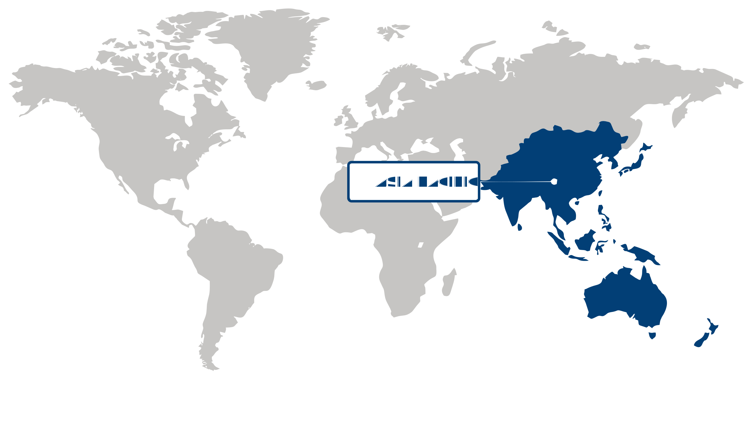
Largest Region
Asia Pacific
Largest Market Share in 2026
Asia Pacific (Largest & Fastest-Growing Region)
The semiconductor pellicle market was led by Asia Pacific, which held the largest share in 2026 while also representing the fastest-growing regional market. The region's strong position is closely linked to its concentration of semiconductor manufacturing, advanced wafer fabrication capabilities, and expanding investments in semiconductor production infrastructure. Growing demand for high-performance and miniaturized electronic devices is encouraging manufacturers to adopt increasingly sophisticated lithography processes, where pellicles play an important role in protecting photomasks from contamination and maintaining process stability. The continued development of advanced semiconductor nodes is further increasing the importance of high-quality pellicle solutions capable of supporting demanding lithography requirements. In addition, the region benefits from an established ecosystem of semiconductor equipment suppliers, materials manufacturers, fabrication facilities, and supporting technology providers, enabling faster adoption of innovations in pellicle design and materials. Government initiatives aimed at strengthening domestic semiconductor capabilities and improving supply-chain resilience are also encouraging investments across the regional semiconductor ecosystem. As fabrication capacity expands and manufacturers increasingly focus on yield improvement, contamination control, and advanced lithography performance, Asia Pacific is expected to maintain its leading position while sustaining strong growth momentum in the semiconductor pellicle market.
Key Country Insights
The U.S. semiconductor pellicle market is driven by investments in advanced semiconductor manufacturing and research into next-generation lithography processes. Companies in the U.S. are focusing on high-transmittance pellicles that support increasingly complex chip fabrication requirements.
Japan plays a critical role in semiconductor pellicles through its strength in high-purity materials and precision manufacturing. Japanese companies are prioritizing advanced pellicle technologies capable of meeting stringent requirements associated with cutting-edge lithography applications.
South Korea's extensive semiconductor manufacturing base supports sustained demand for advanced pellicles in memory chip production. Manufacturers in South Korea are emphasizing defect reduction and compatibility with advanced process nodes to improve production efficiency and yield performance.
Germany's semiconductor pellicle market benefits from its expertise in precision engineering and specialty materials. German suppliers are developing pellicle solutions that address contamination control and process stability requirements for advanced semiconductor production environments.
France is strengthening its semiconductor pellicle capabilities through research initiatives and participation in the European semiconductor ecosystem. Companies in France are focusing on specialty materials and collaborative development programs that support advanced lithography requirements.
Italy's semiconductor pellicle market is influenced by its role in Europe's semiconductor supply chain and precision manufacturing capabilities. Italian companies are pursuing niche opportunities in advanced materials and process components that support contamination control in semiconductor fabrication.
Segment Leadership and Growth Trends
Type Segment Analysis: ArF Pellicle (Largest & Fastest-Growing Segment)
ArF pellicle led the semiconductor pellicle market with a 54.5% share in 2026 and also represented the fastest-growing type segment, reflecting its critical role in protecting photomasks during advanced semiconductor lithography processes. ArF pellicles help prevent particles and contaminants from reaching the mask surface, supporting manufacturing consistency and reducing the risk of pattern defects. Their importance is reinforced by continued semiconductor process refinement and the increasing need for reliable mask protection as fabrication requirements become more demanding. Ongoing improvements in lithography performance and semiconductor manufacturing precision are expected to sustain demand for advanced ArF pellicle solutions.
Application Segment Analysis: IC Foundry (Largest Segment) vs IC Bumping (Fastest-Growing Segment)
The IC foundry segment held the largest share of the semiconductor pellicle market, accounting for 51.94% in 2026, supported by the extensive use of photolithography processes in high-volume semiconductor fabrication. Foundries require effective pellicle solutions to maintain mask cleanliness, improve process reliability, and protect yield during increasingly sophisticated chip manufacturing. IC bumping is expanding more rapidly as advanced packaging and heterogeneous integration gain importance in semiconductor production. The increasing use of sophisticated packaging architectures is strengthening demand for manufacturing processes that require high precision and reliable contamination control throughout fabrication.
| Report Segmentation | |||
| Segment | Sub-Segment | Largest Segment | Fastest Growing Segment |
|---|---|---|---|
| Type | ArF Pellicle, KrF Pellicle, EUV Pellicle, Others | ArF Pellicle | ArF Pellicle |
| Application | IC Bumping, IC Foundry, IC Substrate, MEMS, LED Package | IC Foundry | IC Bumping |
 Read our Research Approach
Competitive Landscape and Market Positioning
Major players in the semiconductor pellicle market:
1. ASML Holding N.V. (Netherlands)
2. Mitsui Chemicals Inc. (Japan)
3. Shin-Etsu Chemical Co. Ltd. (Japan)
4. Toppan Holdings Inc. (Japan)
5. AGC Inc. (Japan)
6. Canatu Oy (Finland)
7. Entegris Inc. (United States)
8. Teledyne DALSA Inc. (Canada)
9. Fujifilm Holdings Corporation (Japan)
10. Micro Lithography Inc. (United States)
The semiconductor pellicle market is advancing through continuous improvements in contamination control and lithography process stability. Material innovation is enhancing durability and performance under extreme manufacturing conditions. Collaborative engineering efforts are enabling next-generation solutions for advanced chip fabrication processes. The semiconductor pellicle market is increasingly driven by precision manufacturing demands and high-end semiconductor scaling requirements.
Why Choose Us
Specialized Expertise: Our team comprises industry experts with a deep understanding of your market segment. We bring specialized knowledge and experience that ensures our research and consulting services are tailored to your unique needs.
Customized Solutions: We understand that every client is different. That's why we offer customized research and consulting solutions designed specifically to address your challenges and capitalize on opportunities within your industry.
Proven Results: With a track record of successful projects and satisfied clients, we have demonstrated our ability to deliver tangible results. Our case studies and testimonials speak to our effectiveness in helping clients achieve their goals.
Cutting-Edge Methodologies: We leverage the latest methodologies and technologies to gather insights and drive informed decision-making. Our innovative approach ensures that you stay ahead of the curve and gain a competitive edge in your market.
Client-Centric Approach: Your satisfaction is our top priority. We prioritize open communication, responsiveness, and transparency to ensure that we not only meet but exceed your expectations at every stage of the engagement.
Continuous Innovation: We are committed to continuous improvement and staying at the forefront of our industry. Through ongoing learning, professional development, and investment in new technologies, we ensure that our services are always evolving to meet your evolving needs.
Value for Money: Our competitive pricing and flexible engagement models ensure that you get maximum value for your investment. We are committed to delivering high-quality results that help you achieve a strong return on your investment.
Select Licence Type