System In Package (SiP) Technology Market Size & Forecasts 2026-2035, By Segments (Interconnection Technology, Packaging Technology, Application), Growth Opportunities, Innovation Landscape, Regulatory Shifts, Strategic Regional Insights (U.S., Japan, China, South Korea, UK, Germany, France), and Competitive Dynamics (TSMC, Samsung Electronics, ASE Technology, Intel, Amkor Technology)
Jump to content
Market Size and Growth Outlook
System In Package Technology Market size is likely to expand from USD 22.72 billion in 2025 to USD 59.47 billion by 2035, posting a CAGR above 10.1% across 2026-2035. The industry’s revenue potential for 2026 is USD 24.73 billion.
Get more details on this report
Request Free Sample ReportSystem In Package (SiP) Technology Market Intelligence Snapshot
Regional Market Dynamics
Segment Momentum
Market Expansion Drivers
Leading Market Participants
Global Market Forecast Snapshot
Market Outlook
Regional and Segment Outlook
Market Growth Drivers and Industry Trends
The surge in wearables, edge IoT and compact consumer devices is driving a premium on footprint and integration, with Apple Inc.’s Apple Watch and AirPods and Samsung Electronics’ wearable lines illustrating device makers prioritizing consolidation. This dynamic shapes the system in package (sip) technology market by prompting OEMs to prefer vendors that deliver RF, power and sensors in single modules. Established OSATs and foundries can expand differentiated SiP service offerings, while fabless designers and specialized start-ups can compete on system-level IP and integration software. Given continued product roadmaps from Apple and Samsung emphasizing miniaturization, supplier collaboration and co-design will increasingly determine procurement decisions.
Technological Advances in SiP Integration and Heterogeneous Packaging
Progress in 2.5D/3D stacking, fan-out and embedded interposers—exemplified by TSMC’s InFO platforms and Intel’s Foveros announcements—lowers thermal and parasitic constraints and enables heterogeneous mixes of logic, memory and RF. That evolution accelerates adoption in the system in package (sip) technology market by enabling higher-function modules for edge AI, 5G and automotive applications. Opportunity exists for TSMC, Intel and OSATs such as ASE Technology Holding and Amkor Technology to capture higher-margin co-design services, while new entrants can differentiate through advanced thermal management, test methodologies and design-for-integration toolchains. Roadmaps published by TSMC and Intel indicate continued technical maturation and ecosystem investments.
Standardization and Regulatory Support for SiP Adoption
Initiatives from JEDEC Solid State Technology Association, the U.S. National Institute of Standards and Technology (NIST) and policy measures such as the European Chips Act reduce integration risk by harmonizing interfaces, testing protocols and qualification pathways, encouraging supply chain investments. Those actions accelerate uptake in the system in package (sip) technology market by shortening qualification cycles for automakers and telecom OEMs. Established suppliers can leverage standards leadership to embed proprietary value chains and obtain government-backed capacity funding, while newcomers can use standardized modules to speed market entry and access public R&D grants. Observable activity in JEDEC working groups and government funding programs is already lowering barriers to commercial deployment.
Industry Restraints:
Thermal and Heterogeneous Integration Complexity
Thermal management and multi-die integration in SiP designs materially slow product cycles because balancing heat dissipation, signal integrity, and testability across stacked logic, memory, and RF dies requires new materials, simulation flows, and qualification regimes. TSMC’s communications on CoWoS/InFO and Intel’s packaging research illustrate the engineering trade-offs and extended validation timelines, while SEMI has highlighted the need for expanded EDA and test ecosystems to support heterogeneous integration. For incumbents this raises R&D and NRE burdens and lengthens time-to-market; for entrants it erects steep technical barriers and dependence on specialist foundries or OSAT partners. Expect this constraint to persist near term, sustaining a premium for firms with advanced integration expertise and driving alliances around shared toolchains and qualification pathways.
OSAT Capacity Concentration and Supply Chain Vulnerabilities
The SiP market is constrained by concentrated advanced-packaging capacity at leading OSATs—ASE Technology, Amkor Technology, and JCET—creating scheduling bottlenecks and supply fragility during demand surges. SEMI and reporting by Reuters during the semiconductor shortage documented extended lead times for packaging services, and attention from the U.S. Department of Commerce via the CHIPS and Science Act underscores geopolitically driven supply-chain risk. Strategically, large OEMs gain priority access through long-term agreements while smaller players face margin pressure and delayed launches. In the medium term, targeted investments and reshoring efforts will increase capacity but geographic redistribution and build-out will take years, leaving near-term bargaining power with established OSATs.
| Growth Driver | Impact on CAGR | Regulatory Influence | Geographic Relevance | Adoption Rate | Impact Timeline |
|---|---|---|---|---|---|
| Demand for miniaturized multi-functional electronics | 3.50% | Short term (≤ 2 yrs) | Asia Pacific, North America | Medium | Fast |
| Technological advances in SiP integration and heterogenous packaging | 4.00% | Medium term (2–5 yrs) | Europe, Asia Pacific | Medium | Moderate |
| Standardization and regulatory support for SiP adoption | 2.50% | Long term (5+ yrs) | North America, Europe | High | Slow |
Unlock insights tailored to your business with our bespoke market research solutions.
Click to get your customized report now.
Regional Demand Dynamics
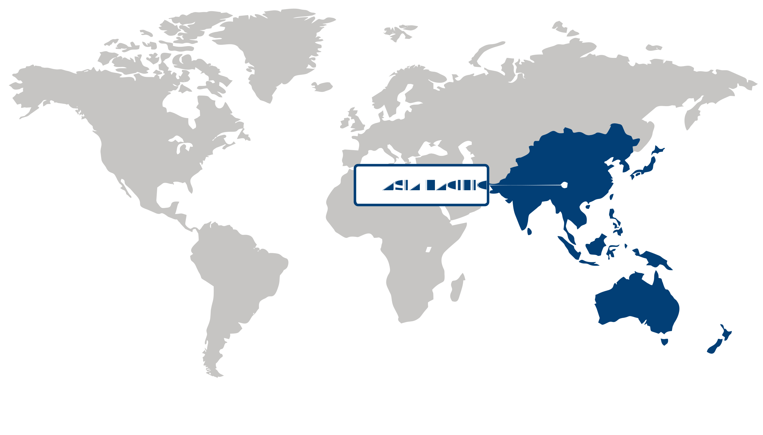
Asia Pacific captured approximately 62.3% of the global system in package (sip) technology market in 2025 and is the largest and fastest-growing region with a 12.12% CAGR. This leadership reflects concentrated electronics manufacturing, the integration of advanced packaging across consumer, telecom, and automotive segments, and major ecosystem investments: TSMC’s advanced packaging roadmaps, Murata Manufacturing Co., Ltd.’s SiP product launches, and policy support signaled by the Ministry of Industry and Information Technology (MIIT) illustrate capacity scaling and technology adoption. Cross-border supply-chain depth, rising onshoring incentives, and strong OEM demand for miniaturization and power efficiency position Asia Pacific as a primary opportunity zone for investors and technology partners.
Japan is positioned as a pivotal hub in Asia Pacific, where the system in package (sip) technology market benefits from specialty materials, precision manufacturing, and targeted industrial policy. Firms such as Murata Manufacturing Co., Ltd. and Renesas Electronics Corporation are advancing compact, high-reliability SiP solutions for automotive and industrial IoT, while the Ministry of Economy, Trade and Industry (METI) programs support domestic packaging capability development. Japan’s strength in substrates, passive components, and quality control creates differentiated, higher-margin nodes within the regional value chain, making it strategically attractive for partners seeking premium SiP applications.
China acts as the production powerhouse in Asia Pacific, with the system in package (sip) technology market scaled by large-volume electronics manufacturing and coordinated capacity expansion. Domestic demand drivers from Huawei and large OEM smartphone/telecom providers, together with capacity moves by Semiconductor Manufacturing International Corporation (SMIC) and ecosystem initiatives highlighted by the China Semiconductor Industry Association (CSIA) and MIIT, are accelerating SiP adoption for cost-optimized, high-density assemblies. For investors and strategists, China offers scale, rapid time-to-market, and an integrated EMS/foundry network that complements Japan’s specialty strengths and reinforces Asia Pacific’s regional dominance.
North America Market Analysis:
North America held a commanding share in the system in package (sip) technology market, driven by deep design ecosystems, high consumer electronics and automotive content per device, and growing advanced-packaging capacity supported by policy and private capital. Large OEMs pressing for miniaturization in wearables and multi-band 5G modules (Apple’s S-series SiP in Apple Watch illustrates end-market pull per Apple press releases) combine with packaging innovation such as Intel’s Foveros and industry commentary from SEMI on rising advanced-packaging demand to sustain leadership. The U.S. Department of Commerce’s CHIPS funding has strengthened local capacity and supply-chain resilience, while industry talent pools and proximity to hyperscalers enable rapid design-to-packaging cycles, making the region attractive for capacity expansions and IP-driven SiP services going forward.
The U.S. serves as the primary driver within North America in the system in package (sip) technology market, where federal incentives, defense and civilian R&D, and large OEM requirements converge. Targeted support under the CHIPS and Science Act administered by the U.S. Department of Commerce, alongside DARPA and NSF-funded packaging research, has catalyzed investments by platform and foundry players (referenced in Department of Commerce announcements and Intel press releases). Strong demand from consumer electronics leaders (Apple’s SiP use) and automotive electrification requirements is translating into procurement and qualification programs that favor U.S.-based assembly/test capacity. Strategic implication: investors aiming at SiP should prioritize partners with U.S. manufacturing footprints and trusted supply-chain credentials to capture OEM qualification pipelines and government-supported programs.
Europe Market Trends:
Europe experienced moderate growth in the system in package (sip) technology market, sustaining a notable presence as policymakers and manufacturers prioritized advanced integration to reduce external dependency. Backing from the European Commission through the EU Chips Act and related funding has spurred capacity and pilot lines, while corporate communications from Infineon Technologies AG and collaborative research by Fraunhofer‑Gesellschaft signal rising industrial adoption. Demand shifts from electrified transport, industrial automation, and edge computing, plus emphasis on supply‑chain resilience, support steady investment. These dynamics position Europe for continued incremental gains and targeted opportunities in tooling, design‑for‑packaging services, and pilot manufacturing.
Germany serves as a leading market in the system in package (sip) technology market, driven chiefly by automotive power electronics and industrial automation demand concentrated around established suppliers and research institutes. Infineon Technologies AG and Bosch have emphasized higher integration for thermal and reliability benefits in recent communications, while Fraunhofer‑Gesellschaft centers in Germany advance heterogeneous integration techniques that lower time‑to‑market. Support from the Federal Ministry for Economic Affairs and Climate Action (BMWK) channels supplier investments into localized packaging capabilities. Strategic implication: Germany’s industrial pull accelerates scale‑up opportunities for regional packaging service providers and materials suppliers.
France acts as an innovation and materials hub in the system in package (sip) technology market, where research centers and substrate suppliers underpin adoption. CEA‑Leti’s prototyping programs and STMicroelectronics’ investments in regional sites, together with Soitec’s silicon‑substrate developments and financing via Bpifrance, create an ecosystem for pilot production and advanced materials qualification. This concentrated R&D‑to‑manufacturing pathway supports commercialization of niche, high‑value SIP solutions and offers regional firms leverage to serve pan‑European automotive and telecom customers.
| Parameter | North America | Asia Pacific | Europe | Latin America | MEA |
|---|---|---|---|---|---|
| Innovation HubiScaleNascentDeveloping Advanced | |||||
| Cost-Sensitive RegioniScaleLowMedium High | |||||
| Regulatory EnvironmentiScaleRestrictiveNeutral Supportive | |||||
| Demand DriversiScaleWeakModerate Strong | |||||
| Development StageiScaleEmergingDeveloping Developed | |||||
| Adoption RateiScaleLowMedium High | |||||
| New Entrants / StartupsiScaleSparseModerate Dense | |||||
| Macro IndicatorsiScaleWeakStable Strong |
System In Package (SiP) Technology Market Share (%), by Interconnection Technology, 2026
Go beyond the chart, access full insights & data tables
Request Free Sample ReportFlip Chip dominated the system in package (sip) technology market in 2025 as the largest share within interconnection technology, driven by rising demand for 2.5-D IC packaging and interposer-based integration required by AI and high-performance computing. Flip chip leadership reflects manufacturing shifts toward dense, low-inductance connections and aligns with customer preference for high-bandwidth, compact modules; TSMC’s CoWoS and Intel’s EMIB implementations and ASE Group press releases illustrate industry adoption. This segment creates strategic advantages for assembly specialists and foundries to offer differentiated interposer services and for startups to innovate on thermal and yield solutions. Given continued investment in heterogenous integration and supply-chain scaling, flip chip is set to remain central in the near to medium term.
Analysis by Packaging Technology
2.5-D IC Packaging represented largest share in 2025 in the system in package (sip) technology market among packaging technology segments because it delivers higher bandwidth and compact form factors demanded by AI, 5G and advanced computing. Adoption is validated by TSMC’s CoWoS roadmaps and AMD/Xilinx product integrations that prioritize interposer-based bandwidth; these examples show how ecosystem partners and design houses favor 2.5-D for performance-density tradeoffs. Opportunities exist for established OSATs to expand interposer capacity and for niche players to offer specialized substrates or thermal solutions. With ongoing advances in interposer materials, test standards and collaboration between foundries and packaging houses, 2.5-D packaging will remain strategically relevant.
Analysis by Application
Consumer Electronics held largest share in 2025 in the system in package (sip) technology market within application segments, propelled by demand for compact, power-efficient packaging in smartphones, wearables and tablets. Apple’s use of SiP in the Apple Watch and Samsung Electronics’ emphasis on compact module integration exemplify how consumer device makers prioritize miniaturization and battery efficiency; Qualcomm ecosystem announcements also signal supplier alignment. This creates advantages for integrated device manufacturers and agile OSATs to co-develop tailored SiP solutions for form-factor-sensitive products. As consumer demand for smaller, smarter devices and regulatory focus on energy efficiency continue, consumer electronics will sustain strong relevance through the near to medium term.
| Segment | Sub-Segment | Largest Segment | Fastest Growing |
|---|---|---|---|
| Interconnection Technology | Wire Bond, Flip Chip | ||
| Packaging Technology | 2-D IC Packaging, 2.5-D IC Packaging, 3-D IC Packaging | ||
| Application | Consumer Electronics, Automotive, Telecommunication, Industrial System, Aerospace & Defense, Others |
Competitive Landscape and Market Positioning
The competitive environment is marked by value-chain alignment and capability stacking among these incumbents: strategic ties to design houses and foundries, targeted capacity reshaping, rollout of advanced heterogeneous integration modules, and sustained investment in packaging process and thermal/interconnect R&D. Such activity narrows differentiation to specialized integration know-how and system-level IP, pressures mid-tier players to specialize or consolidate, and elevates the importance of end-market customization (automotive, 5G/AI, consumer) for commercial traction. Market positioning now hinges on speed of integration and breadth of turnkey SiP solutions.
Strategic / Actionable Recommendations for Regional Players
Players embedded in strong design ecosystems and hyperscale/cloud demand should deepen cooperative development with platform OEMs, prioritize SiP variants optimized for heterogeneous compute and high-density interconnects, and deploy pilot assembly capabilities and IP for thermal management to capture adjacent system revenue.
Organizations located within dense manufacturing and OSAT clusters ought to leverage proximity to foundries by extending joint development of wafer-to-package flows, scaling substrate and interposer capabilities, and forging supply partnerships that shorten time-to-market for telecom and mobile SiP modules.
Groups serving markets with strict reliability and automotive requirements should focus on certifiable process flows, modular SiP offerings tailored to automotive and industrial specs, and selective alliances with tier-one vehicle and industrial OEMs to secure high-margin, long-lifecycle opportunities.
| Company | Market Share | Company Revenue | Revenue CAGR (%) | Product Portfolio | Geographic Presence | Innovation / R&D Focus | Strategic Developments |
|---|---|---|---|---|---|---|---|
| No companies available. | |||||||
Customize Your Report
Explore examples of how this report can be tailored to different research needs, including custom segments, additional topics or chapters, and related reports. Click a section of the wheel or its numbered marker to explore the available options.
System In Package (SiP) Technology Market — Custom Segments
| Segment | Sub-Segment |
|---|---|
| No segment data available. | |
System In Package (SiP) Technology Market — Custom TOC
| Custom Chapter | Chapter Details |
|---|---|
| No custom TOC data available. | |
Need a different cut of the data?
Request Custom ResearchFrequently Asked Questions
How much is the system in package technology market worth?
How will the system in package (SiP) technology industry grow in terms of size and CAGR by 2035?
Which region shows the largest market footprint in the system in package (SiP) technology market?
Which region leads in terms of year-over-year growth for the system in package technology sector?
Why does flip chip sub-segment dominate the interconnection technology segment of system in package (SiP) technology sector?
How much is the 2.5-D IC packaging segment expected to grow in the system in package (SiP) technology industry beyond 2025?
What factors give consumer electronics segment a competitive edge in the system in package (SiP) technology sector?
What are the key competitors in the system in package (SiP) technology landscape?
Our Clients
"Working with FBI has been a good experience. The market report provided a holistic view, covering everything from emerging trends to potential risks."
Semtech Corporation
"The experience was highly positive. The team showcased remarkable flexibility in adapting to our specific needs and delivered report that perfectly aligned with all our requirements."
TSMC
"What really stood out to me was how clearly and promptly the Fundamental Business Insights team communicated throughout. It made the collaboration feel effortless."
NXP Semiconductors
Our Research Team & Methodology
Every Fundamental Business Insights report is built by a dedicated vertical research team, validated through a structured primary-and-secondary methodology, and reviewed for accuracy before it reaches you.
Delivery
Published
Available
Support
- Market Size & Forecast
- Market Segmentation
- Regional Analysis
- Growth Drivers & Challenges
- Market Dynamics
- Competitive Landscape
- Company Profiles
- Competitive Benchmarking
- Mergers & Acquisitions
- Market Share Analysis or Key Company Strategies
- Value Chain Analysis
- Porter's Five Forces
- PESTLE Analysis
- Pricing Trends
- Supply-Demand Analysis
- Technology Landscape
- Regulatory Landscape
- Investment & Funding Landscape
- Emerging Opportunities
- Future Market Outlook