Topological Insulators Market Size & Growth Forecast 2027–2036, By Segments (Type, Application), Regional Demand Trends (North America, Asia Pacific, Europe), Key Country Insights (U.S., Japan, South Korea, Germany, France, Italy), and Competitive Landscape
Jump to Content
Market Size and Growth Outlook
Topological Insulators Market size was more than USD 557.08 million in 2026 and is set to grow at a 9.22% CAGR between 2027 and 2036, crossing USD 1.35 billion by 2036. The industry revenue for 2027 is calculated at USD 600.7 million.
Get more details on this report
Request Free Sample ReportTopological Insulators Market Intelligence Snapshot
Regional Market Dynamics
- North America accounted for 36.5% of the market in 2026, supported by advanced materials research, semiconductor capabilities, and investment in quantum technologies and next-generation electronics.
- Growing research into quantum materials, spintronics, and next-generation computing is supporting regional growth, while academic collaborations and advanced materials investment strengthen research and development capabilities.
Segment Momentum
- 2D topological insulators represented 82.81% of market revenue in 2026, supported by research into atomically thin materials for nanoelectronics, spintronics, quantum devices, and advanced sensing. Their tunable electronic properties and compatibility with layered architectures strengthen their research and development appeal.
- 3D topological insulators are expected to grow at the fastest rate as researchers explore their distinctive surface-state transport and quantum properties for spintronics, quantum computing, and sensing. Progress in material synthesis and device fabrication is supporting further development.
Market Expansion Drivers
- Rising research in quantum computing and spintronics.
- Development of advanced materials and fabrication techniques.
- Expansion of industrial applications in electronics and sensors.
Leading Market Participants
- Top companies in the topological insulators market include 2D Semiconductors (USA), HQ Graphene B.V. (Netherlands), American Elements (USA), MKNano (USA), SixCarbon Technology (China), Stanford Advanced Materials (USA), Nano Research Elements (USA), Heeger Materials Inc. (USA), Otto Chemie Pvt. Ltd. (India), SPINTEC (France).
Global Market Forecast Snapshot
Market Outlook
- 2026 Market Size: USD 557.08 million
- 2027 Estimated Market Size: USD 600.7 million
- Projected Market Size: USD 1.35 billion by 2036
- Growth Forecast: 9.22% CAGR (2027-2036)
Regional and Segment Outlook
- Leading Regional Market: North America
- High-Growth Regional Hub: Europe
- Core Revenue Segment: Type (2D Topological Insulators) | Application (Electronics & Semiconductors)
- Emerging Opportunity Segment: Type (3D Topological Insulators) | Application (Electronics & Semiconductors)
Market Growth Drivers and Industry Trends
Rising research in quantum computing and spintronics
The rising research in quantum computing and spintronics is expected to drive demand for topological insulators due to their distinctive electronic and spin-related properties. Researchers are exploring these materials for applications involving low-power information processing, quantum states, and advanced electronic architectures. Increasing interest in next-generation computing technologies and novel approaches to controlling electronic and spin transport is expected to strengthen research and development activities involving topological materials.
Development of advanced materials and fabrication techniques
The development of advanced materials and fabrication techniques is supporting market growth by improving the ability to produce and characterize topological insulators with desirable electronic properties. Progress in material engineering, thin-film deposition, nanostructuring, and device fabrication is enabling researchers to address challenges associated with material quality and practical integration. Continued advancements in manufacturing and experimental techniques are expected to expand the feasibility of incorporating topological materials into emerging technological applications.
Expansion of industrial applications in electronics and sensors
The expansion of industrial applications in electronics and sensors is creating growth opportunities for topological insulators as their unique conductivity, surface-state behavior, and sensitivity to external conditions attract interest for advanced device development. Research into next-generation sensing, electronic components, and energy-efficient devices is increasing the potential application scope of these materials. Growing efforts to translate laboratory-scale material advances into practical electronic and sensing technologies are expected to support broader market development.
| Growth Driver | Impact on CAGR | Regulatory Influence | Geographic Relevance | Adoption Rate | Impact Timeline |
|---|---|---|---|---|---|
| Rising research in quantum computing and spintronics | 3.5% | Short term (≤ 2 yrs) | North America; Europe; Spillover: Asia Pacific | Medium | Moderate |
| Development of advanced materials and fabrication techniques | 3% | Medium term (2–5 yrs) | Europe; Asia Pacific; Spillover: North America | Medium | Moderate |
| Expansion of industrial applications in electronics and sensors | 2.5% | Long term (5+ yrs) | North America; Asia Pacific; Spillover: Europe | Low | Moderate |
Explore Growth Opportunities
Request Free Sample ReportRegional Demand Dynamics
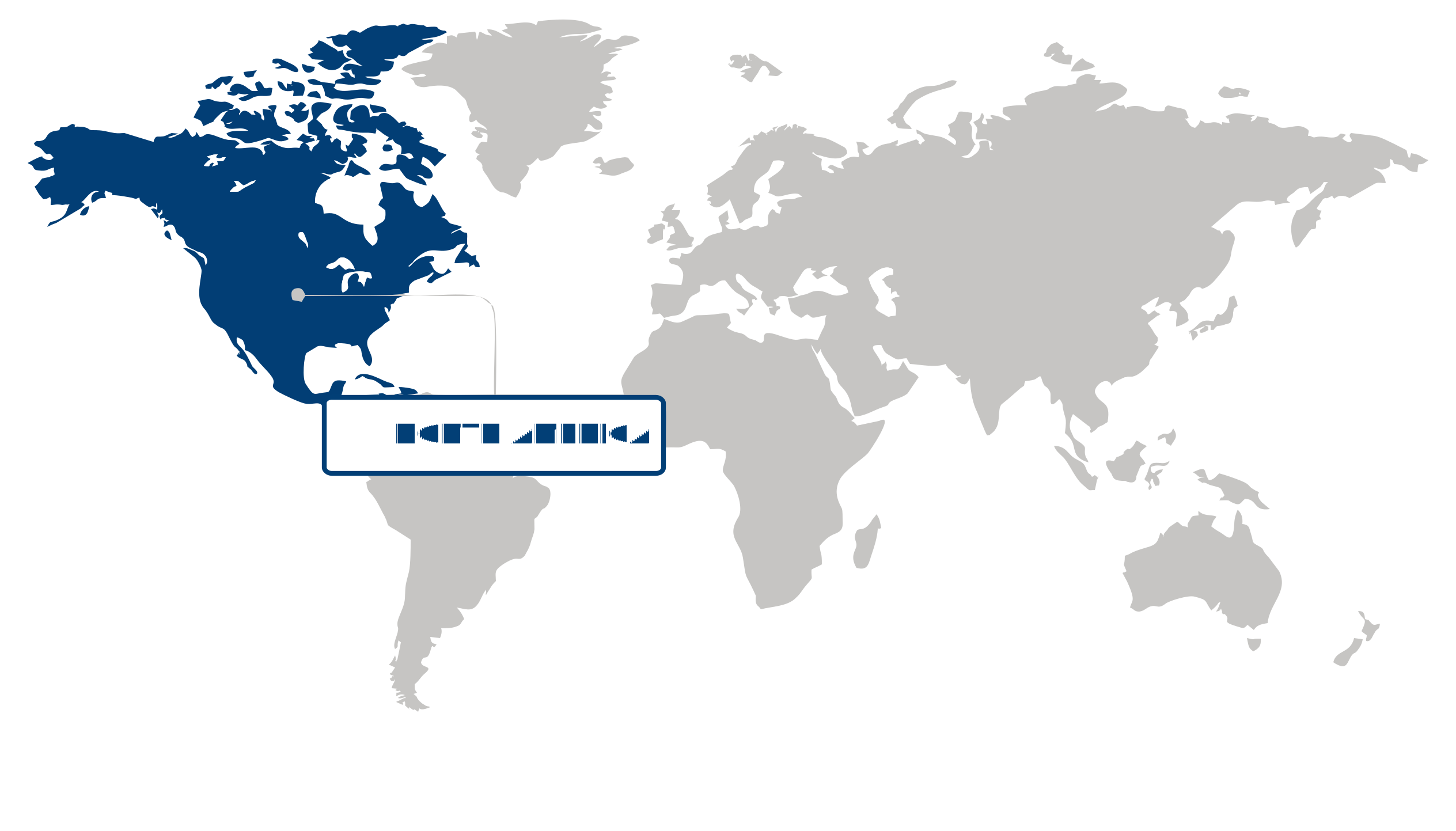
North America (Largest Region)
North America accounted for a 36.5% share in 2026 and maintained its position as the largest regional market, backed by strong research capabilities in condensed matter physics, advanced materials science, and semiconductor technologies. Increasing research into quantum materials and novel electronic properties is driving interest in topological insulators for applications associated with next-generation electronics, spintronics, quantum computing, and advanced sensing technologies. Strong collaboration between academic institutions, research organizations, and technology-focused industries is supporting continued innovation in material synthesis, characterization, and device development. Growing investments in advanced semiconductor research and quantum technologies are further strengthening regional capabilities. These developments are reinforcing North America’s leading role in the development and commercialization potential of topological insulator technologies.
Europe (Fastest-Growing Region)
Europe is anticipated to be the fastest-growing region, driven by increasing research activity in quantum materials, advanced electronics, and next-generation computing technologies. Growing interest in the unique electronic and quantum properties of topological insulators is encouraging research into their potential applications in spintronics, quantum devices, and low-power electronic systems. Strong academic and scientific research networks are supporting advances in material discovery, fabrication, and characterization, while increasing attention to quantum technologies is creating additional opportunities for topological materials. Investments in advanced materials research and collaborative scientific programs are further strengthening the regional ecosystem.
| Parameter | North America | Asia Pacific | Europe | Latin America | MEA |
|---|---|---|---|---|---|
| Innovation HubiScaleNascentDeveloping Advanced | |||||
| Cost-Sensitive RegioniScaleLowMedium High | |||||
| Regulatory EnvironmentiScaleRestrictiveNeutral Supportive | |||||
| Demand DriversiScaleWeakModerate Strong | |||||
| Development StageiScaleEmergingDeveloping Developed | |||||
| Adoption RateiScaleLowMedium High | |||||
| New Entrants / StartupsiScaleSparseModerate Dense | |||||
| Macro IndicatorsiScaleWeakStable Strong |
Key Country Insights
United States 🇺🇸
Quantum Materials ResearchThe U.S. is prioritizing topological insulators through advanced materials research, quantum technology programs, and next-generation electronic applications. Commercial activity centers on improving material quality, scalable fabrication, and integration into spintronic, quantum, and low-power device architectures as research moves toward practical prototypes.
Germany 🇩🇪
Materials Engineering FocusGermany is emphasizing topological insulators within precision materials science and advanced semiconductor research. Priorities include reproducible material synthesis, characterization, and integration with nanoscale devices, particularly where topological properties can contribute to spintronics, quantum components, and energy-efficient electronics.
Japan 🇯🇵
Quantum Device IntegrationJapan is exploring topological insulators for advanced electronic and quantum-device architectures, supported by strong capabilities in materials engineering and semiconductor research. Development priorities include controlling surface-state properties, improving fabrication consistency, and translating laboratory materials into specialized low-power and spin-based devices.
South Korea 🇰🇷
Semiconductor Application DevelopmentSouth Korea is connecting topological-insulator research with its broader semiconductor and advanced electronics ecosystem. Key priorities include scalable thin-film production, interface engineering, and integration into spintronic and quantum-device platforms where distinctive electronic properties can provide functionality beyond conventional semiconductor materials.
France 🇫🇷
Fundamental Materials InnovationFrance is advancing topological-insulator research through fundamental condensed-matter physics and specialized materials development. Commercial relevance is increasingly tied to translating experimental discoveries into reproducible materials and device structures for quantum information, spintronics, and other emerging electronic applications.
Italy 🇮🇹
Specialized Materials ResearchItaly is focusing on specialized topological-material research spanning synthesis, characterization, and nanoscale device experimentation. Near-term priorities include improving material stability and understanding electronic behavior to support potential applications in spintronics, quantum technologies, and advanced sensing architectures.
Topological Insulators Market Share (%), by Type, 2026
Go beyond the chart, access full insights & data tables
Request Free Sample ReportType Segment Analysis: 2D Topological Insulators (Largest Segment) vs 3D Topological Insulators (Fastest-Growing Segment)
The 2D topological insulators segment dominated the topological insulators market, accounting for the largest revenue share of 82.81% in 2026, supported by growing research and development interest in atomically thin materials that exhibit distinctive electronic properties and can be integrated into advanced nanoscale technologies. Their reduced dimensionality, tunable electronic characteristics, and compatibility with thin-film and layered material architectures make 2D topological insulators relevant to emerging applications in nanoelectronics, spintronics, quantum devices, and advanced sensing technologies. The ability to engineer their properties through material composition, thickness, interfaces, and external stimuli is also encouraging continued investigation across both academic and industrial research environments. Increasing interest in low-power electronic architectures and next-generation materials is further supporting their relevance, while advances in fabrication and characterization techniques are improving the feasibility of developing practical devices based on 2D topological materials.
The 3D topological insulators segment is expected to register the fastest growth, driven by increasing interest in materials that combine insulating bulk behavior with conductive surface states and their potential application in advanced electronic and quantum technologies. Three-dimensional topological systems provide a broader material platform for investigating robust surface-state transport, spin-related phenomena, and unconventional electronic behavior, creating opportunities across spintronics, quantum computing, sensing, and other emerging applications. Continued progress in material synthesis, surface engineering, and device fabrication is helping researchers address challenges associated with defects, bulk conductivity, and interface quality. As demand grows for materials capable of enabling new approaches to information processing and electronic functionality, 3D topological insulators are attracting greater attention for applications that require distinctive surface transport and quantum properties.
Application Segment Analysis: Electronics & Semiconductors (Largest & Fastest-Growing Segment)
The electronics & semiconductors application segment dominated the topological insulators market, accounting for the largest revenue share of 44.1% in 2026, while also representing the fastest-growing application segment. Its strong position is driven by the potential of topological materials to enable new electronic architectures with distinctive charge and spin transport characteristics. Topological insulators are being explored for applications involving spintronic devices, low-power electronics, advanced sensors, and other semiconductor technologies where conventional materials may face limitations in performance, energy efficiency, or scalability. Their unusual surface-state behavior provides opportunities to develop devices that exploit controlled electron transport and spin-related properties, supporting continued research into next-generation semiconductor components. Increasing demand for miniaturized, energy-efficient, and high-performance electronic systems is further encouraging exploration of advanced materials that can provide differentiated functionality. As fabrication techniques improve and integration challenges are progressively addressed, electronics and semiconductor applications are expected to remain a key area for the development and commercialization of topological-insulator-based technologies.
| Segment | Sub-Segment | Largest Segment | Fastest Growing |
|---|---|---|---|
| Type | 3D Topological Insulators, 2D Topological Insulators | 2D Topological Insulators | 3D Topological Insulators |
| Application | Electronics & Semiconductors, Telecommunications, Defense & Aerospace, Medical Devices, Others | Electronics & Semiconductors | Electronics & Semiconductors |
Unlock insights tailored to your business with our bespoke market research solutions.
Click to get your customized report now.
Competitive Landscape and Market Positioning
Analyst Perspective:
Competition in the topological insulators market remains largely research-driven, with material quality, fabrication reproducibility, and device integration shaping progress toward commercialization. Potential applications in spintronics and quantum technologies depend on translating distinctive electronic properties into measurable performance advantages over established materials. Wafer-scale thin-film growth is a critical challenge, as variations in composition, thickness, and crystal structure can undermine consistency across devices. Demonstrating stable topological states at room temperature and preserving these properties during fabrication are equally important for practical applications. Although low-power and high-speed electronic components represent promising areas of investigation, commercial viability requires repeatable manufacturing, reliable interfaces, and validated device-level benefits. Collaboration between material developers and device researchers remains important to addressing these interconnected technical barriers.
Major players in the topological insulators market:
- 2D Semiconductors (USA)
- HQ Graphene B.V. (Netherlands)
- American Elements (USA)
- MKNano (USA)
- SixCarbon Technology (China)
- Stanford Advanced Materials (USA)
- Nano Research Elements (USA)
- Heeger Materials Inc. (USA)
- Otto Chemie Pvt. Ltd. (India)
- SPINTEC (France)
| Company | Market Share | Company Revenue | Revenue CAGR (%) | Product Portfolio | Geographic Presence | Innovation / R&D Focus | Strategic Developments |
|---|---|---|---|---|---|---|---|
| 2D Semiconductors (USA) | |||||||
| HQ Graphene B.V. (Netherlands) | |||||||
| American Elements (USA) | |||||||
| MKNano (USA) | |||||||
| SixCarbon Technology (China) | |||||||
| Stanford Advanced Materials (USA) | |||||||
| Nano Research Elements (USA) | |||||||
| Heeger Materials Inc. (USA) | |||||||
| Otto Chemie Pvt. Ltd. (India) | |||||||
| SPINTEC (France) |
Industry Development/News
| Company Name | Date | Key Development |
|---|---|---|
| Korea Research Institute of Standards and Science (KRISS) | August 2026 | Korea Research Institute of Standards and Science, alongside research partners, successfully resolved the mechanism behind unexplained signal behaviors in topological insulators. The breakthrough establishes a fundamental benchmarking standard for signal processing, directly improving the design predictability, material evaluation, and commercial reliability of topological-insulator-based quantum electronic devices. |
| Microsoft | February 2025 | Microsoft, through its Station Q research unit, unveiled Majorana 1, an eight-qubit topological quantum processor built on a newly engineered topological superconductor material. The system leverages exotic Majorana zero modes to achieve hardware-level error resilience, marking a critical milestone in scaling topological quantum computing architectures and commercializing advanced topological materials. |
| INOX Group | October 2024 | INOX Group collaborated with the Indian Institute of Science to establish a dedicated Quantum Materials Lab focusing on topological semiconductors. The initiative includes manufacturing commercial-grade domestic Molecular Beam Epitaxy equipment, significantly advancing regional supply chain capabilities, infrastructure development, and commercial fabrication capacity for topological insulator materials. |
Customize Your Report
Explore examples of how this report can be tailored to different research needs, including custom segments, additional topics or chapters, and related reports. Click a section of the wheel or its numbered marker to explore the available options.
Topological Insulators Market — Custom Segments
| Segment | Sub-Segment |
|---|---|
| Material Platform | Bismuth-Based Compounds, Antimony-Based Compounds, Mercury-Based Compounds, Rare-Earth-Based Compounds |
| Fabrication Method | Molecular Beam Epitaxy, Physical Vapor Deposition & Sputtering, Chemical Vapor Deposition, Bulk Crystal Growth |
| Commercialization Stage | Research & Laboratory Stage, Pilot & Pre-Commercial Stage, Commercial Deployment |
Topological Insulators Market — Custom TOC
| Custom Chapter | Chapter Details |
|---|---|
| Commercialization Readiness Assessment |
|
| Quantum Technology Application Roadmap |
|
| Research-to-Industry Translation |
|
Need a different cut of the data?
Request Custom ResearchFrequently Asked Questions
How large is the topological insulators market?
How will the topological insulators industry grow in terms of size and CAGR by 2036?
How are quantum computing and spintronics research shaping demand for topological insulators?
How are advances in fabrication techniques supporting commercialization opportunities for topological insulators?
Why do 2D topological insulators account for the largest market share?
What is driving the growth of 3D topological insulators?
Why does North America hold the largest share of the topological insulators market?
What is accelerating topological insulators market growth in Europe?
Who are the leading players in the topological insulators landscape?
Our Clients
"Working with FBI has been a good experience. The market report provided a holistic view, covering everything from emerging trends to potential risks."
Semtech Corporation
"The experience was highly positive. The team showcased remarkable flexibility in adapting to our specific needs and delivered report that perfectly aligned with all our requirements."
TSMC
"What really stood out to me was how clearly and promptly the Fundamental Business Insights team communicated throughout. It made the collaboration feel effortless."
NXP Semiconductors
Our Research Team & Methodology
Every Fundamental Business Insights report is built by a dedicated vertical research team, validated through a structured primary-and-secondary methodology, and reviewed for accuracy before it reaches you.
This report was prepared by the Electronics & Semiconductors Research Team at Fundamental Business Insights, a dedicated research group specializing in the global electronics and semiconductor ecosystem. Our analysts continuously monitor technology innovations, manufacturing trends, competitive developments, supply chain dynamics, regulatory changes, and end-user demand to deliver timely market intelligence. The research is developed using a structured methodology that combines primary industry interactions, company financial disclosures, government publications, trade associations, technical literature, patent analysis, and other authoritative secondary sources. Market estimates are validated through multiple research techniques, including top-down and bottom-up analysis, before undergoing an internal quality review to ensure accuracy, consistency, and methodological integrity prior to publication.
Delivery
Published
Available
Support
- Market Size & Forecast
- Market Segmentation
- Regional Analysis
- Growth Drivers & Challenges
- Market Dynamics
- Competitive Landscape
- Company Profiles
- Competitive Benchmarking
- Mergers & Acquisitions
- Market Share Analysis or Key Company Strategies
- Value Chain Analysis
- Porter's Five Forces
- PESTLE Analysis
- Pricing Trends
- Supply-Demand Analysis
- Technology Landscape
- Regulatory Landscape
- Investment & Funding Landscape
- Emerging Opportunities
- Future Market Outlook