


Compound Semiconductor Market Size & Growth Forecast 2027–2036, By Segments (Product, Deposition Technologies, Type, Application), Regional Demand Trends (North America, Asia Pacific, Europe), Key Country Insights (U.S., Japan, South Korea, Germany, France, Italy), and Competitive Landscape
Market Size and Growth Outlook
Compound Semiconductor Market size was over USD 48.79 Billion in 2026 and is likely to grow at 10.61% CAGR between 2027 and 2036, reaching USD 133.74 Billion by 2036. The industry revenue for 2027 is assessed at USD 53.27 Billion.
Base Year Value (2026)
USD 48.79 Billion
CAGR (2027-2036)
10.61%
Forecast Year Value (2036)
USD 133.74 Billion

Historical Data Period
2022-2026

Largest Region
North America

Forecast Period
2027-2036
Compound Semiconductor Market Intelligence Snapshot:
-
Regional Market Dynamics:
- North America held 33.05% in 2025, supported by semiconductor research capabilities, advanced telecommunications infrastructure, and demand across aerospace, defense, automotive, communications, and high-performance computing.
- Asia Pacific is projected to grow fastest through expanding electronics manufacturing, communication infrastructure, semiconductor investments, and rising demand from electric mobility, 5G, and energy-efficient systems.
-
Segment Momentum:
- The LED segment led the market in 2025 due to strong adoption in lighting, automotive, displays, and signage, supported by growing demand for energy-efficient illumination and continuous performance improvements.
- Silicon Carbide (SiC) is growing the fastest as demand rises for energy-efficient, high-power semiconductor devices used in electric vehicles, renewable energy systems, and industrial power electronics.
-
Market Expansion Drivers:
- Rapid expansion of EVs and renewable energy systems driving compound semiconductor demand
- 5G and high-frequency network rollout accelerating adoption of compound semiconductor materials
- Growing photonics and radar applications enabling advanced sensing and communication system integration
-
Leading Market Participants:
Top players in the compound semiconductor market include Infineon Technologies AG (Germany), Qorvo, Inc. (USA), Skyworks Solutions, Inc. (USA), Wolfspeed, Inc. (USA), STMicroelectronics N.V. (Switzerland), Texas Instruments Incorporated (USA), ams-OSRAM AG (Austria), MACOM Technology Solutions Holdings, Inc. (USA), Samsung Electronics Co., Ltd. (South Korea), Sumitomo Electric Industries, Ltd. (Japan)
Global Market Forecast Snapshot:
-
Market Outlook:
- 2026 Market Size: USD 48.79 Billion
- 2027 Estimated Market Size: USD 53.27 Billion
- Projected Market Size: USD 133.74 Billion by 2036
- Growth Forecasts: 10.61% CAGR (2027-2036)
-
Regional and Segment Outlook:
- Leading Regional Market: North America
- High-Growth Regional Hub: Asia Pacific
- Core Revenue Segment: LED (Product) | Chemical Vapor Deposition (CVD) (Deposition Technologies) | Gallium Arsenide (GAAS) (Type) | Telecommunication (Application)
- Emerging Opportunity Segment: Power Electronics (Product) | Atomic Layer Deposition (ALD) (Deposition Technologies) | Silicon Carbide (SiC) (Type) | Datacom (Application)
Market Growth Drivers and Industry Trends
Rapid expansion of EVs and renewable energy systems driving compound semiconductor demand
The accelerating transition toward electric mobility and clean energy generation is increasing demand for semiconductor materials capable of supporting high-efficiency power conversion and thermal performance. This shift will drive the compound semiconductor market growth as electric vehicles, charging infrastructure, solar power systems, and energy storage applications increasingly rely on advanced materials that deliver higher power density and lower energy losses. Manufacturers are adopting these semiconductors to improve system efficiency, extend operating life, and enable more compact designs for next-generation energy technologies.
5G and high-frequency network rollout accelerating adoption of compound semiconductor materials
Global deployment of advanced wireless communication infrastructure is creating strong demand for electronic components that perform efficiently at higher frequencies and power levels. The compound semiconductor market benefits from expanding 5G networks because these materials offer superior electrical characteristics required for radio frequency amplifiers, base stations, and high-speed communication equipment. Their ability to support faster signal transmission, improved energy efficiency, and reliable operation under demanding network conditions makes them increasingly important for modern telecommunications infrastructure.
Growing photonics and radar applications enabling advanced sensing and communication system integration
Rapid innovation in optical communication, industrial sensing, aerospace, automotive electronics, and defense technologies is broadening the adoption of advanced semiconductor materials. Expanding use of these technologies will propel the compound semiconductor market growth by increasing demand for materials that enable high-performance photonic devices, radar systems, lasers, and precision sensing applications. Their exceptional electronic and optical properties support accurate signal generation, efficient light emission, and reliable high-frequency operation across increasingly sophisticated communication and sensing platforms.
| Growth Driver Assessment Framework | |||||
| Growth Driver | Impact On CAGR | Regulatory Influence | Geographic Relevance | Adoption Rate | Impact Timeline |
|---|---|---|---|---|---|
| Rapid expansion of EVs and renewable energy systems driving compound semiconductor demand | 3.1% | High | Asia Pacific, Europe, North America | High | Near Term |
| 5G and high-frequency network rollout accelerating adoption of compound semiconductor materials | 2.8% | High | Asia Pacific, North America | High | Near Term |
| Growing photonics and radar applications enabling advanced sensing and communication system integration | 2.5% | Moderate | Europe, North America | High | Mid Term |
Unlock insights tailored to your business with our bespoke market research solutions - Click to get your customized report now!
Regional Demand Dynamics
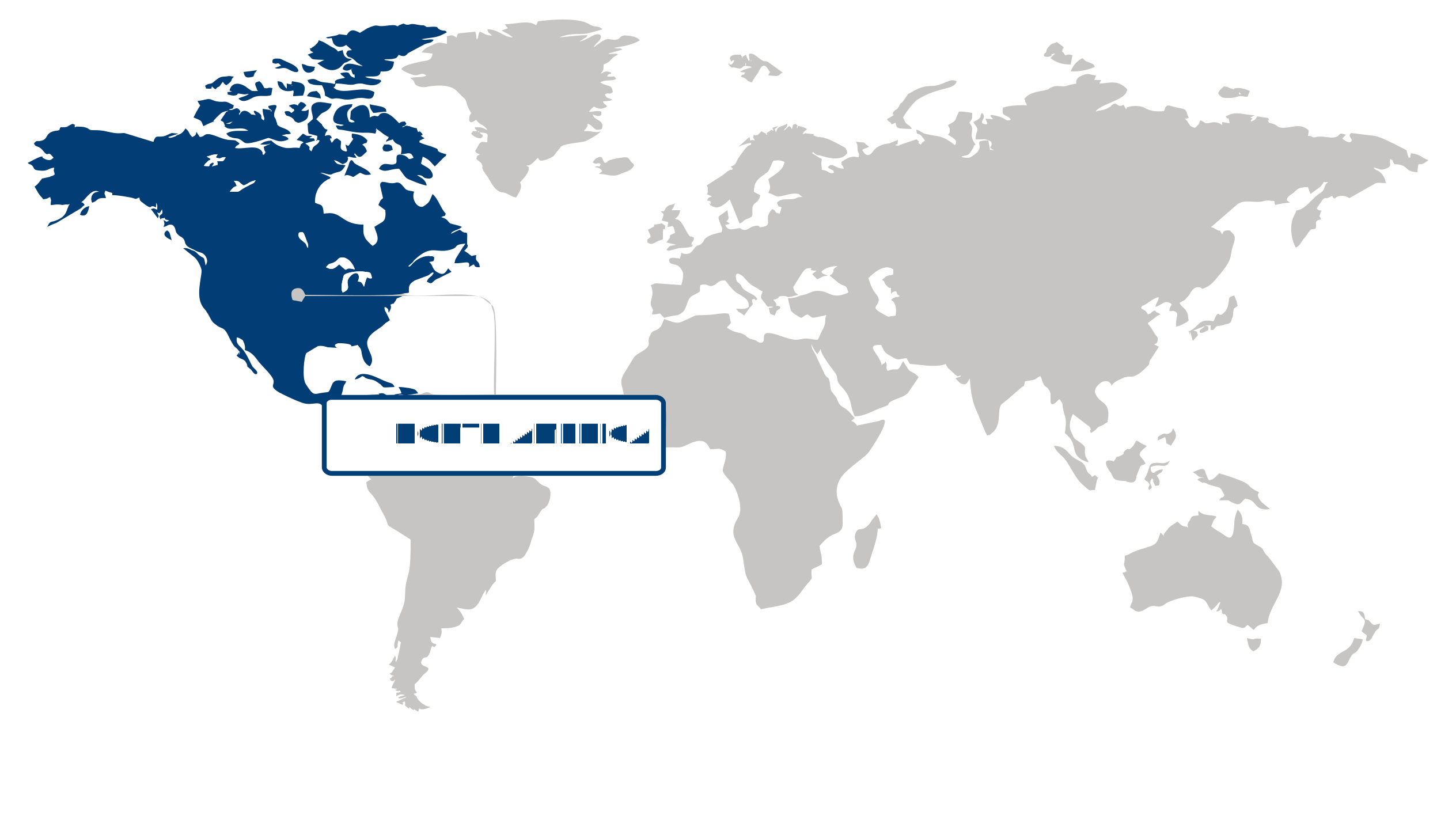
Largest Region
North America
33.05% Market Share in 2026
North America (Largest Region) vs Asia Pacific (Fastest-Growing Region)
North America held the largest share of the compound semiconductor market, accounting for 33.05% in 2026. The region’s strong position is supported by established semiconductor research capabilities, advanced telecommunications infrastructure, and broad adoption of compound semiconductor materials across aerospace, defense, automotive, communications, and high-performance computing applications. Growing demand for high-frequency, high-power, and energy-efficient electronic components is encouraging investment in advanced semiconductor technologies, while continued development of next-generation wireless networks and sophisticated electronic systems is sustaining regional demand.
Asia Pacific is projected to represent the fastest-growing regional market, driven by expanding electronics manufacturing, increasing deployment of advanced communication infrastructure, and rising demand for high-performance semiconductor components. The region’s extensive consumer electronics and automotive production base provides a broad application environment for compound semiconductors, particularly in power electronics, radio-frequency devices, and optoelectronic systems. Continued investment in semiconductor manufacturing capabilities and the development of electric mobility, 5G networks, and energy-efficient electronic systems are further strengthening the region’s growth prospects.
No card data available for this language/report.
Segment Leadership and Growth Trends
Product Segment Analysis: LED (Largest Segment) vs Power Electronics (Fastest-Growing Segment)
The LED segment held the largest share in 2026, supported by the extensive adoption of compound semiconductors in general lighting, automotive lighting, display technologies, and signage applications. Strong demand for energy-efficient illumination solutions and continuous improvements in LED performance have sustained the segment's dominant position. The broad commercialization of LED technology across residential, industrial, and commercial sectors further reinforces its market leadership.
The compound semiconductor market is expected to witness the fastest growth in the power electronics segment due to increasing demand for high-efficiency power conversion and energy management solutions. The expanding adoption of electric vehicles, renewable energy systems, and advanced industrial equipment is accelerating the use of compound semiconductor-based power devices. Their ability to operate efficiently under high temperatures and voltages continues to support rapid market expansion.
Deposition Technologies Segment Analysis: Chemical Vapor Deposition (CVD) (Largest Segment) vs Atomic Layer Deposition (ALD) (Fastest-Growing Segment)
Chemical vapor deposition (CVD) accounted for the largest segment in 2026, owing to its widespread use in producing high-quality semiconductor layers with excellent uniformity and scalability. The technology remains a preferred manufacturing process for a broad range of compound semiconductor devices because it supports high-volume production while delivering consistent material characteristics. Its established industrial adoption continues to underpin the segment's leading position.
Atomic layer deposition (ALD) is anticipated to register the fastest growth as semiconductor manufacturers increasingly require ultra-thin, highly uniform films for next-generation electronic and optoelectronic devices. The technology's exceptional precision and ability to deposit conformal coatings on complex structures make it increasingly valuable for advanced semiconductor fabrication. Continued miniaturization and higher device performance requirements are driving broader implementation of ALD processes.
Type Segment Analysis: Gallium Arsenide (GAAS) (Largest Segment) vs Silicon Carbide (SiC) (Fastest-Growing Segment)
Gallium arsenide (GaAs) emerged as the largest segment in 2026, reflecting its extensive application in high-frequency communication devices, optoelectronics, and radio frequency components. Its superior electron mobility and excellent performance in high-speed applications have made GaAs a preferred material for advanced communication technologies and specialized electronic devices. Continued deployment of high-performance wireless infrastructure has further strengthened its market position.
In the compound semiconductor market, the silicon carbide (SiC) segment is projected to witness the fastest growth due to increasing demand for high-power and high-temperature semiconductor devices. SiC enables greater energy efficiency and improved thermal performance, making it particularly attractive for electric mobility, renewable energy systems, and industrial power electronics. Ongoing advancements in energy-efficient technologies continue to accelerate the adoption of silicon carbide-based devices.
| Report Segmentation | |||
| Segment | Sub-Segment | Largest Segment | Fastest Growing Segment |
|---|---|---|---|
| Product | LED, Optoelectronics, RF Devices, Power Electronics | LED | Power Electronics |
| Deposition Technologies | Chemical Vapor Deposition (CVD), Molecular Beam Epitaxy, Hydride Vapor Phase Epitaxy (HVPE), Ammonothermal, Liquid Phase Epitaxy, Atomic Layer Deposition (ALD), Others | Chemical Vapor Deposition (CVD) | Atomic Layer Deposition (ALD) |
| Type | GaN, Gallium Arsenide (GAAS), Silicon Carbide (SiC), Indium Phosphide (INP), Silicon Germanium (SIGE), Gallium Phosphide (GAP), Others | Gallium Arsenide (GAAS) | Silicon Carbide (SiC) |
| Application | General Lighting, Telecommunication, Military, Defense and Aerospace, Automotive, Power Supply, Datacom, Consumer Display, Commercial, Consumer Devices, Others | Telecommunication | Datacom |
 Read our Research Approach
Competitive Landscape and Market Positioning
Key companies in the compound semiconductor market:
- Infineon Technologies AG (Germany)
- Qorvo, Inc. (USA)
- Skyworks Solutions, Inc. (USA)
- Wolfspeed, Inc. (USA)
- STMicroelectronics N.V. (Switzerland)
- Texas Instruments Incorporated (USA)
- ams-OSRAM AG (Austria)
- MACOM Technology Solutions Holdings, Inc. (USA)
- Samsung Electronics Co., Ltd. (South Korea)
- Sumitomo Electric Industries Ltd. (Japan)
Technological capability has become the principal arena of competition in the compound semiconductor market as manufacturers pursue materials and fabrication processes that deliver superior performance for high-frequency, high-power, and optoelectronic applications. Success increasingly depends on mastering sophisticated production techniques while maintaining consistent wafer quality and supporting the demanding specifications of advanced electronic systems. The market is also witnessing stronger alignment between material innovation and end-use application development, prompting suppliers to deepen engineering collaboration with device manufacturers and accelerate the commercialization of next-generation semiconductor architectures that address rapidly evolving performance requirements.
Industry Development/News
| Company Name | Date | Key Development |
|---|---|---|
| GCCS | May-26 | GCCS signed a joint development agreement with Purdue University to scale silicon carbide (SiC) substrates to 8-inch and 12-inch formats. The operational initiative optimizes thermal performance to clear supply chain bottlenecks for next-generation 6G chips and AI data centers. |
| Crystal Matrix | May-26 | Crystal Matrix secured government approval to build an integrated compound semiconductor fabrication and advanced packaging facility in Gujarat. The project establishes foundational domestic manufacturing footprint under India's multi-billion dollar semiconductor incentive program. |
| IQE | Apr-26 | IQE secured an £81 million strategic investment led by Macom. The funding strengthens IQE’s capital structure and expands its high-volume compound semiconductor manufacturing facilities to support market demand for advanced epitaxial wafers in optical and wireless communications. |
| AIXTRON | Mar-26 | AIXTRON finalized plans to establish a new manufacturing facility in Malaysia. The geographic expansion scales the company's production capacity for specialized compound semiconductor metal-organic chemical vapor deposition (MOCVD) equipment to meet rising global manufacturing demand. |
| SiCSem | Nov-25 | SiCSem broke ground on a ₹2,500 crore commercial silicon carbide (SiC) fabrication plant in Odisha, India, in partnership with Clas-SiC Wafer Fab. The facility will manufacture 60,000 wafers annually, targeting supply chain insertion for electric vehicles, solar inverters, and defense systems. |
| Coherent | Aug-25 | Coherent operationalized a new silicon carbide (SiC) manufacturing facility in Vietnam. The facility expands the company's global supply chain and production footprint for wide-bandgap substrate materials, addressing rising demand in industrial and automotive applications. |
| Navitas Semiconductor | May-25 | Navitas Semiconductor commercialized a high-efficiency 12 kW power supply architecture utilizing its Gen-3 SiC MOSFETs and GaNSafe integrated circuits. Achieving 97.8% efficiency, the system targets immediate technology adoption in energy-intensive hyperscale AI data centers. |
| Vanguard International Semiconductor | Nov-24 | Vanguard International Semiconductor entered a joint partnership with Episil to construct an 8-inch silicon carbide (SiC) wafer fabrication facility. This collaboration accelerates the transition from 6-inch to 8-inch manufacturing scales, driving down production costs for automotive power electronics. |
| STMicroelectronics | May-24 | STMicroelectronics unveiled plans to construct a fully integrated silicon carbide (SiC) manufacturing facility in Catania, Italy. The multi-billion euro investment spans the entire SiC value chain from substrate production to device fabrication, securing long-term supply chain resilience for electric vehicles. |
| Vishay | Mar-24 | Vishay finalized the acquisition of Newport Wafer Fab for $177 million. The transaction transforms Vishay’s manufacturing capabilities by adding a large-scale automotive-certified wafer fabrication facility to its portfolio, directly enhancing its competitive positioning in power compound semiconductors. |
Why Choose Us
Specialized Expertise: Our team comprises industry experts with a deep understanding of your market segment. We bring specialized knowledge and experience that ensures our research and consulting services are tailored to your unique needs.
Customized Solutions: We understand that every client is different. That's why we offer customized research and consulting solutions designed specifically to address your challenges and capitalize on opportunities within your industry.
Proven Results: With a track record of successful projects and satisfied clients, we have demonstrated our ability to deliver tangible results. Our case studies and testimonials speak to our effectiveness in helping clients achieve their goals.
Cutting-Edge Methodologies: We leverage the latest methodologies and technologies to gather insights and drive informed decision-making. Our innovative approach ensures that you stay ahead of the curve and gain a competitive edge in your market.
Client-Centric Approach: Your satisfaction is our top priority. We prioritize open communication, responsiveness, and transparency to ensure that we not only meet but exceed your expectations at every stage of the engagement.
Continuous Innovation: We are committed to continuous improvement and staying at the forefront of our industry. Through ongoing learning, professional development, and investment in new technologies, we ensure that our services are always evolving to meet your evolving needs.
Value for Money: Our competitive pricing and flexible engagement models ensure that you get maximum value for your investment. We are committed to delivering high-quality results that help you achieve a strong return on your investment.
Select Licence Type