EUV Pellicle Market Size & Growth Forecast 2027–2036, By Segments (Material, Application), Regional Demand Trends (North America, Asia Pacific, Europe), Key Country Insights (U.S., Japan, South Korea, Germany, France, Italy), and Competitive Landscape
Jump to Content
Market Size and Growth Outlook
EUV Pellicle Market size was more than USD 702.96 million in 2026 and is set to grow at a 14.98% CAGR between 2027 and 2036, reaching USD 2.84 billion by 2036. The industry revenue for 2027 is calculated at USD 794.06 million.
Get more details on this report
Request Free Sample ReportEUV Pellicle Market Intelligence Snapshot
Regional Market Dynamics
- Asia Pacific accounted for 62.69% of market revenue in 2026, supported by its strong semiconductor manufacturing ecosystem, advanced chip production investments, and increasing adoption of extreme ultraviolet lithography.
- Asia Pacific leads market growth as advanced-node manufacturing expands, semiconductor fabrication investments increase, and chip complexity drives demand for reliable pellicles that protect photomasks during advanced lithography.
Segment Momentum
- Carbon-based materials held a 93.1% market share in 2026 due to their thermal stability, mechanical strength, and high EUV transmittance, supporting photomask protection, imaging accuracy, and improved wafer yields.
- Semiconductor foundries accounted for 57.94% of the market in 2026 and are the fastest-growing application segment, driven by advanced chip production, increasing EUV lithography adoption, and the need to reduce contamination-related defects.
Market Expansion Drivers
- Rising demand for advanced semiconductor manufacturing.
- Advancements in EUV pellicle materials & durability.
- Expansion of semiconductor fabs in emerging regions.
Leading Market Participants
- Major companies in the EUV pellicle market include Mitsui Chemicals (Japan), ASML (Netherlands), Shin-Etsu Chemical (Japan), Fujifilm (Japan), SKC (South Korea), Samsung Electronics (South Korea), Toppan (Japan), Sumitomo Chemical (Japan), LG Chem (South Korea), DuPont (USA).
Global Market Forecast Snapshot
Market Outlook
- 2026 Market Size: USD 702.96 million
- 2027 Estimated Market Size: USD 794.06 million
- Projected Market Size: USD 2.84 billion by 2036
- Growth Forecast: 14.98% CAGR (2027-2036)
Regional and Segment Outlook
- Leading Regional Market: Asia Pacific
- High-Growth Regional Hub: Asia Pacific
- Core Revenue Segment: Material (Carbon-based) | Application (Semiconductor Foundries)
- Emerging Opportunity Segment: Material (Carbon-based) | Application (Semiconductor Foundries)
Market Growth Drivers and Industry Trends
Rising demand for advanced semiconductor manufacturing
The growing need for advanced semiconductor manufacturing is driving demand for EUV pellicles that protect photomasks from contamination during extreme ultraviolet lithography processes. As semiconductor production moves toward increasingly sophisticated process technologies, manufacturers require highly reliable pellicle solutions capable of preserving mask cleanliness and supporting consistent pattern transfer, making pellicle performance an increasingly important factor in advanced lithography workflows.
Advancements in EUV pellicle materials & durability
Continuous advancements in EUV pellicle materials are supporting market growth by addressing the demanding requirements of extreme ultraviolet exposure, thermal stability, transmission, mechanical strength, and durability. Improvements in material composition and structural design are enabling pellicles to withstand repeated lithography processes while maintaining optical performance, helping semiconductor manufacturers improve process reliability and reduce risks associated with mask contamination and pellicle degradation.
Expansion of semiconductor fabs in emerging regions
The expansion of semiconductor fabrication capacity across emerging regions is creating additional demand for advanced lithography components, including EUV pellicles. New and upgraded fabrication facilities are increasing the need for sophisticated contamination-control and mask-protection technologies, while the development of regional semiconductor ecosystems is supporting greater adoption of specialized EUV infrastructure and associated consumables required for advanced chip manufacturing.
| Growth Driver | Impact on CAGR | Regulatory Influence | Geographic Relevance | Adoption Rate | Impact Timeline |
|---|---|---|---|---|---|
| Rising demand for advanced semiconductor manufacturing | 5% | Short term (≤ 2 yrs) | North America; Asia Pacific; Spillover: Europe | Medium | Fast |
| Advancements in EUV pellicle materials & durability | 4% | Medium term (2–5 yrs) | Asia Pacific; North America | Medium | Moderate |
| Expansion of semiconductor fabs in emerging regions | 3% | Long term (5+ yrs) | Asia Pacific; Europe; Spillover: North America | Low | Moderate |
Explore Growth Opportunities
Request Free Sample ReportRegional Demand Dynamics
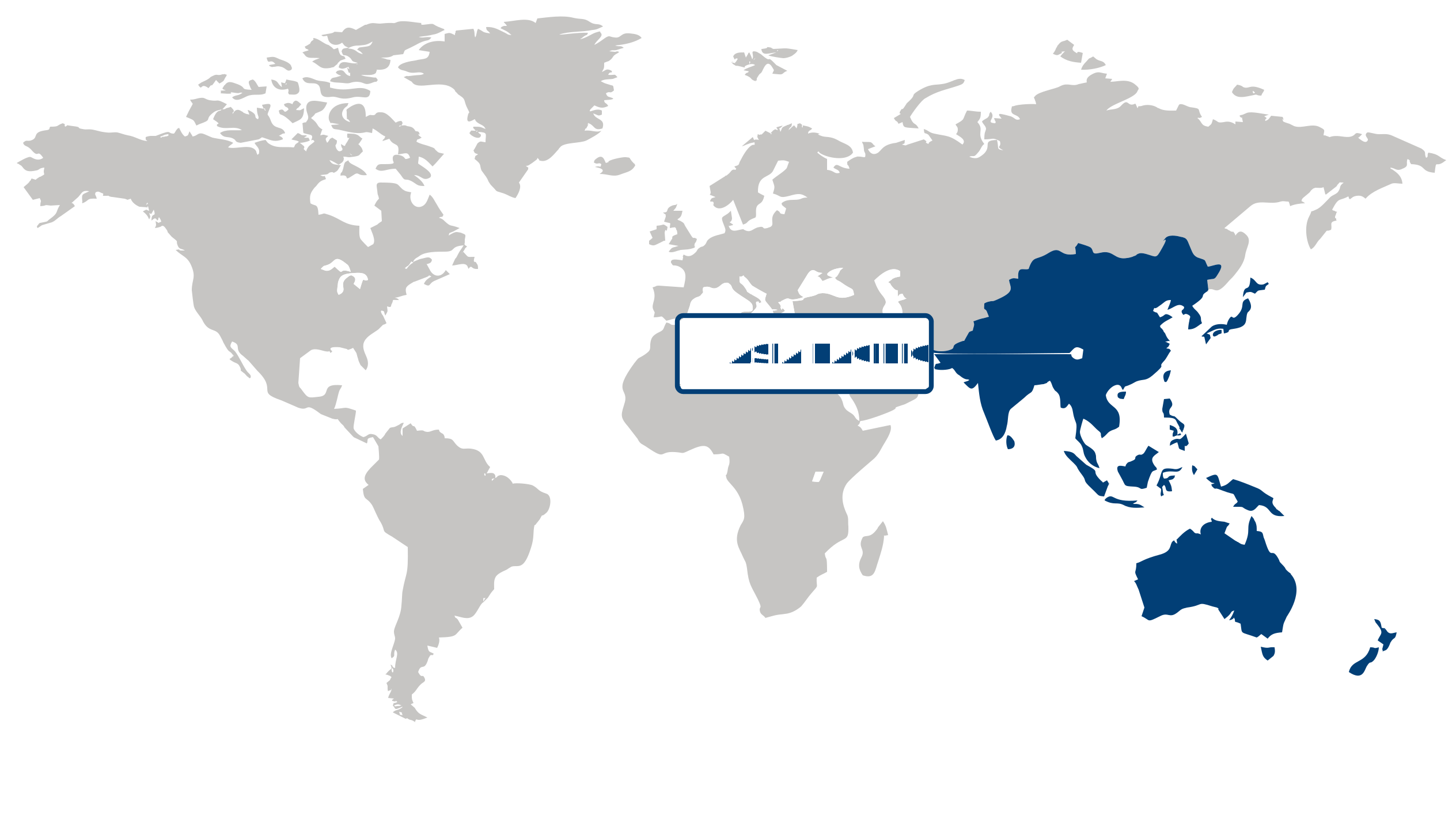
Asia Pacific (Largest & Fastest-Growing Region)
Asia Pacific held the largest revenue share of 62.69% in 2026 and is also the fastest-growing region in the EUV pellicle market, supported by the region’s strong semiconductor manufacturing ecosystem, expanding advanced chip production capabilities, and increasing adoption of extreme ultraviolet lithography. The growing complexity of semiconductor devices is creating greater demand for highly reliable pellicles that can protect photomasks while maintaining lithography performance during advanced manufacturing processes. Continued investment in semiconductor fabrication infrastructure and the expansion of advanced-node production are strengthening the need for sophisticated lithography materials and components. The region’s established electronics manufacturing base, expanding semiconductor research capabilities, and focus on improving domestic supply chains are further supporting the development and adoption of EUV pellicle technologies.
| Parameter | North America | Asia Pacific | Europe | Latin America | MEA |
|---|---|---|---|---|---|
| Innovation HubiScaleNascentDeveloping Advanced | |||||
| Cost-Sensitive RegioniScaleLowMedium High | |||||
| Regulatory EnvironmentiScaleRestrictiveNeutral Supportive | |||||
| Demand DriversiScaleWeakModerate Strong | |||||
| Development StageiScaleEmergingDeveloping Developed | |||||
| Adoption RateiScaleLowMedium High | |||||
| New Entrants / StartupsiScaleSparseModerate Dense | |||||
| Macro IndicatorsiScaleWeakStable Strong |
Key Country Insights
United States 🇺🇸
Advanced Lithography EcosystemThe U.S. EUV pellicle market is supported by semiconductor equipment innovation and advanced lithography research. Priorities center on improving pellicle transmission, durability, defect control, and thermal performance as chipmakers pursue tighter process tolerances and higher EUV exposure efficiency.
Germany 🇩🇪
Precision Materials EngineeringGermany contributes advanced materials and precision-engineering capabilities relevant to EUV pellicle development. Market priorities include defect minimization, thin-film performance, and manufacturing consistency, with suppliers focused on meeting increasingly demanding requirements for semiconductor lithography components and high-purity production environments.
Japan 🇯🇵
Pellicle Manufacturing ExpertiseJapan has strong capabilities across semiconductor materials and pellicle-related manufacturing technologies. Commercial priorities include developing highly transmissive, mechanically robust membranes and improving defect control, while suppliers work closely with lithography stakeholders to meet the demanding specifications of next-generation EUV semiconductor processes.
South Korea 🇰🇷
High-Volume Chip IntegrationSouth Korea’s semiconductor manufacturing base creates practical demand for EUV pellicles that can withstand high-volume fabrication conditions. Priorities include durability, contamination control, transmission stability, and process compatibility, particularly as advanced logic and memory manufacturers expand EUV adoption across increasingly sophisticated production nodes.
France 🇫🇷
EUV Research CapabilityFrance’s role in EUV pellicles is connected to advanced semiconductor research, materials science, and precision manufacturing capabilities. Key priorities involve membrane development, optical transmission, thermal stability, and reliable fabrication processes that can support European participation in increasingly complex EUV lithography supply chains.
Italy 🇮🇹
Precision Component DevelopmentItaly’s opportunity in EUV pellicles is concentrated around specialized materials, precision components, and semiconductor manufacturing technologies. Suppliers can target niche requirements involving thin-film fabrication, dimensional control, and process reliability, particularly where advanced lithography equipment demands increasingly specialized supporting components.
EUV Pellicle Market Share (%), by Material, 2026
Go beyond the chart, access full insights & data tables
Request Free Sample ReportMaterial Segment Analysis: Carbon-based (Largest & Fastest-Growing Segment)
Carbon-based materials held a 93.1% share of the EUV pellicle market in 2026, driven by their superior thermal stability, high mechanical strength, and ability to withstand the demanding operating conditions of extreme ultraviolet lithography. Carbon-based materials are widely utilized in EUV pellicles due to their high EUV transmittance, low thickness, and resistance to thermal degradation, enabling effective protection of photomasks during advanced semiconductor manufacturing. Their ability to minimize particle contamination, maintain imaging accuracy, and support consistent lithographic performance makes them essential for producing high-precision semiconductor devices. The increasing adoption of advanced lithography processes for manufacturing smaller, more complex, and energy-efficient chips is further strengthening demand for carbon-based EUV pellicles. The segment is also expected to register the fastest growth, supported by the growing need for advanced semiconductor fabrication technologies, increasing investments in next-generation manufacturing facilities, and the rising demand for high-performance computing, artificial intelligence, and advanced electronic devices. Additionally, ongoing research into improving carbon-based membrane durability, EUV transmission efficiency, thermal resistance, and mechanical reliability is enhancing their suitability for increasingly demanding lithography applications. The growing focus on reducing defect rates, improving wafer yields, and maintaining stringent manufacturing precision is further encouraging semiconductor manufacturers to adopt advanced carbon-based pellicle solutions, supporting the segment's continued expansion.
Application Segment Analysis: Semiconductor Foundries (Largest & Fastest-Growing Segment)
The semiconductor foundries segment held a 57.94% share of the EUV pellicle market in 2026, driven by the extensive use of extreme ultraviolet lithography in advanced semiconductor fabrication and the growing demand for high-precision photomask protection. Semiconductor foundries rely on EUV pellicles to prevent particle contamination and minimize defects during complex lithographic processes, supporting consistent wafer quality and improved manufacturing yields. The increasing production of advanced logic chips, high-performance processors, and specialized semiconductor components is strengthening the adoption of EUV pellicles across foundry operations. As semiconductor manufacturing continues to advance toward increasingly sophisticated process technologies, the need for reliable pellicle materials with high EUV transmittance, thermal stability, and mechanical durability is becoming increasingly important. The segment is also expected to register the fastest growth, supported by rising investments in advanced fabrication facilities, increasing demand for semiconductors used in artificial intelligence, data centers, automotive electronics, and high-performance computing, and the continued expansion of EUV lithography applications. The growing complexity of semiconductor manufacturing processes is encouraging foundries to adopt advanced contamination-control solutions to improve production efficiency and reduce defect-related losses. Furthermore, continuous advancements in pellicle membrane design, manufacturing precision, and thermal management are supporting the development of more reliable EUV pellicles. The increasing focus on improving wafer yields, maintaining process stability, and supporting high-volume production of advanced semiconductor devices is expected to further drive demand for EUV pellicles among semiconductor foundries.
| Segment | Sub-Segment | Largest Segment | Fastest Growing |
|---|---|---|---|
| Material | Silicon-based, Carbon-based | Carbon-based | Carbon-based |
| Application | Semiconductor Foundries, Memory Devices, Consumer Electronics, Others | Semiconductor Foundries | Semiconductor Foundries |
Unlock insights tailored to your business with our bespoke market research solutions.
Click to get your customized report now.
Competitive Landscape and Market Positioning
Analyst Perspective:
Commercial viability in the EUV pellicle market hinges on bridging the gap between prototype material innovation and high-volume manufacturing yields. While high-transmission carbon nanotube membranes, polysilicon, and metal-free alternatives offer unique trade-offs across optical clarity, thermal endurance, and mechanical stability, laboratory success alone does not guarantee adoption. Suppliers differentiate themselves by proving extreme thermal and power durability under grueling, real-world exposure conditions where failure threatens costly lithography operations. Ultimately, competitive leadership depends on achieving process reproducibility, stringent defect control, and high yield rates while ensuring seamless integration into existing mask-handling workflows.
Key companies in the EUV pellicle market:
- Mitsui Chemicals (Japan)
- ASML (Netherlands)
- Shin-Etsu Chemical (Japan)
- Fujifilm (Japan)
- SKC (South Korea)
- Samsung Electronics (South Korea)
- Toppan (Japan)
- Sumitomo Chemical (Japan)
- LG Chem (South Korea)
- DuPont (USA)
| Company | Market Share | Company Revenue | Revenue CAGR (%) | Product Portfolio | Geographic Presence | Innovation / R&D Focus | Strategic Developments |
|---|---|---|---|---|---|---|---|
| Mitsui Chemicals (Japan) | |||||||
| ASML (Netherlands) | |||||||
| Shin-Etsu Chemical (Japan) | |||||||
| Fujifilm (Japan) | |||||||
| SKC (South Korea) | |||||||
| Samsung Electronics (South Korea) | |||||||
| Toppan (Japan) | |||||||
| Sumitomo Chemical (Japan) | |||||||
| LG Chem (South Korea) | |||||||
| DuPont (USA) |
Industry Development/News
| Company Name | Date | Key Development |
|---|---|---|
| Samsung | March 2026 | Samsung accelerated the operational ramp-up of its Taylor facility, initiating trial runs for extreme ultraviolet (EUV) lithography tools. The milestone indicates that domestically produced EUV pellicles could integrate into the U.S. production line, supporting the company's broader expansion of advanced manufacturing and lithography capabilities. |
| Samsung | June 2025 | Samsung and blank mask manufacturer S&S Tech jointly filed a patent for extreme ultraviolet (EUV) pellicles. The co-filing establishes collaborative research and development efforts aimed at advancing pellicle component technologies to support upcoming extreme ultraviolet lithography manufacturing processes. |
| TSMC | February 2025 | TSMC repurposed its discontinued 8-inch Fab 3 in Hsinchu Science Park to establish in-house production for extreme ultraviolet (EUV) pellicles. This strategic manufacturing expansion internalizes the production of protective membranes used alongside EUV photomasks, altering the company's supply chain integration and component sourcing framework. |
| Imec | December 2023 | Imec and Mitsui Chemicals entered into a strategic partnership to commercialize carbon nanotube (CNT) pellicle technology for extreme ultraviolet (EUV) lithography. The collaboration focuses on leveraging CNT pellicles to deliver enhanced transmittance, thermal resistance, and mechanical durability, accelerating advanced pellicle adoption for next-generation semiconductor manufacturing ecosystems. |
Customize Your Report
Explore examples of how this report can be tailored to different research needs, including custom segments, additional topics or chapters, and related reports. Click a section of the wheel or its numbered marker to explore the available options.
EUV Pellicle Market — Custom Segments
| Segment | Sub-Segment |
|---|---|
| Wafer Node | 7 nm and Above, 5–6 nm, 3–4 nm, 2 nm and Below |
| Manufacturing Stage | Prototype & Development, Qualification, High-Volume Manufacturing |
EUV Pellicle Market — Custom TOC
| Custom Chapter | Chapter Details |
|---|---|
| EUV Pellicle Supply Chain Resilience |
|
| Semiconductor Fab Adoption Pathways |
|
| Pellicle Cost-of-Ownership and Mask Protection Economics |
|
Need a different cut of the data?
Request Custom ResearchFrequently Asked Questions
How big is the EUV pellicle market?
How is the EUV pellicle industry expected to grow over the next 10 years?
How is advanced semiconductor manufacturing influencing EUV pellicle demand?
Why are EUV pellicle material advancements strategically important for semiconductor manufacturers?
Why do carbon-based materials dominate the EUV pellicle market?
Why are semiconductor foundries driving demand for EUV pellicles?
Why does Asia Pacific dominate the EUV pellicle market?
What is accelerating EUV pellicle market growth in Asia Pacific?
Who are the leading players in the EUV pellicle landscape?
Our Clients
"Working with FBI has been a good experience. The market report provided a holistic view, covering everything from emerging trends to potential risks."
Semtech Corporation
"The experience was highly positive. The team showcased remarkable flexibility in adapting to our specific needs and delivered report that perfectly aligned with all our requirements."
TSMC
"What really stood out to me was how clearly and promptly the Fundamental Business Insights team communicated throughout. It made the collaboration feel effortless."
NXP Semiconductors
Our Research Team & Methodology
Every Fundamental Business Insights report is built by a dedicated vertical research team, validated through a structured primary-and-secondary methodology, and reviewed for accuracy before it reaches you.
This report was prepared by the Electronics & Semiconductors Research Team at Fundamental Business Insights, a dedicated research group specializing in the global electronics and semiconductor ecosystem. Our analysts continuously monitor technology innovations, manufacturing trends, competitive developments, supply chain dynamics, regulatory changes, and end-user demand to deliver timely market intelligence. The research is developed using a structured methodology that combines primary industry interactions, company financial disclosures, government publications, trade associations, technical literature, patent analysis, and other authoritative secondary sources. Market estimates are validated through multiple research techniques, including top-down and bottom-up analysis, before undergoing an internal quality review to ensure accuracy, consistency, and methodological integrity prior to publication.
Delivery
Published
Available
Support
- Market Size & Forecast
- Market Segmentation
- Regional Analysis
- Growth Drivers & Challenges
- Market Dynamics
- Competitive Landscape
- Company Profiles
- Competitive Benchmarking
- Mergers & Acquisitions
- Market Share Analysis or Key Company Strategies
- Value Chain Analysis
- Porter's Five Forces
- PESTLE Analysis
- Pricing Trends
- Supply-Demand Analysis
- Technology Landscape
- Regulatory Landscape
- Investment & Funding Landscape
- Emerging Opportunities
- Future Market Outlook