Semiconductor Bonding Equipment Market Size & Growth Forecast 2027–2036, By Segments (Equipment Type, Bonding Type, End Use Industry, Application), Regional Demand Trends (North America, Asia Pacific, Europe), Key Country Insights (U.S., Japan, South Korea, Germany, France, Italy), and Competitive Landscape
Market Size and Growth Outlook
Semiconductor Bonding Equipment Market size was over USD 2.43 Billion in 2026 and is likely to grow at 9.01% CAGR between 2027 and 2036, crossing USD 5.76 Billion by 2036. The industry revenue for 2027 is assessed at USD 2.62 Billion.
Get more details on this report
Request Free Sample ReportSemiconductor Bonding Equipment Market Intelligence Snapshot
Regional Market Dynamics
- Asia Pacific held 56.65% in 2026, supported by concentrated semiconductor manufacturing, advanced packaging investment, fabrication expansion, and demand for sophisticated chip assembly.
- High-performance computing, artificial intelligence, consumer electronics, and automotive semiconductors are increasing production complexity and demand for precise bonding equipment.
Segment Momentum
- Wire bonding equipment held the largest share at 42.12% in 2026, driven by its manufacturing reliability, cost efficiency, and compatibility with high-volume semiconductor packaging applications.
- The automotive segment is growing fastest as vehicles incorporate more electronics, advanced driver assistance systems, electric powertrains, and connected technologies, increasing demand for advanced semiconductor bonding equipment.
Market Expansion Drivers
- Expansion of semiconductor manufacturing driving advanced chip bonding and packaging equipment demand
- Growing EV and 5G deployment increasing need for high-performance semiconductor interconnect solutions
- Rising investment in advanced packaging technologies enabling heterogeneous integration and miniaturized chips
Leading Market Participants
- Key players in the semiconductor bonding equipment market include Applied Materials, Inc. (United States), Tokyo Electron Limited (Japan), ASMPT Limited (Hong Kong), Kulicke and Soffa Industries, Inc. (United States), BE Semiconductor Industries N.V. (Netherlands), EV Group (EVG) (Austria), SUSS MicroTec SE (Germany), Nidec Corporation (Japan), Canon Inc. (Japan), Panasonic Connect Co., Ltd. (Japan)
Global Market Forecast Snapshot
Market Outlook
- 2026 Market Size: USD 2.43 Billion
- 2027 Estimated Market Size: USD 2.62 Billion
- Projected Market Size: USD 5.76 Billion by 2036
- Growth Forecast: 9.01% CAGR (2027-2036)
Regional and Segment Outlook
- Leading Regional Market: Asia Pacific
- High-Growth Regional Hub: Asia Pacific
- Core Revenue Segment: Wire Bonding Equipment (Equipment Type) | Permanent Bonding (Bonding Type) | Consumer Electronics (End Use Industry) | Advanced Packaging (Application)
- Emerging Opportunity Segment: Wafer Bonding Equipment (Equipment Type) | Hybrid Bonding (Bonding Type) | Automotive (End Use Industry) | Photonic Devices (Application)
Market Growth Drivers and Industry Trends
Expansion of semiconductor manufacturing driving advanced chip bonding and packaging equipment demand
The continued expansion of semiconductor fabrication capacity is increasing the need for advanced assembly technologies, which will drive the semiconductor bonding equipment market growth. As chip production volumes rise, manufacturers require highly precise bonding systems capable of supporting efficient packaging processes while maintaining stringent quality standards. Advanced bonding equipment enables accurate die attachment, wafer-level integration, and reliable interconnections that are essential for producing increasingly sophisticated semiconductor devices across multiple end-use industries.
Growing EV and 5G deployment increasing need for high-performance semiconductor interconnect solutions
Rising adoption of electric vehicles and next-generation communication infrastructure is creating stronger demand for advanced semiconductor devices, supporting the semiconductor bonding equipment market. High-performance electronic components used in power management, wireless communication, sensing, and computing applications require reliable bonding technologies that ensure efficient electrical connectivity and long-term operational stability. As semiconductor performance requirements continue to increase, manufacturers invest in precision bonding solutions capable of meeting tighter design tolerances and higher production efficiency.
Rising investment in advanced packaging technologies enabling heterogeneous integration and miniaturized chips
Increasing emphasis on advanced semiconductor packaging is encouraging wider adoption of sophisticated bonding equipment, which will propel the semiconductor bonding equipment market growth. Heterogeneous integration combines multiple chip technologies within compact packages to improve processing capability, energy efficiency, and functional performance while supporting continued device miniaturization. Advanced bonding systems provide the alignment accuracy and process control necessary for assembling complex package architectures that accommodate higher component densities and evolving semiconductor design requirements.
| Growth Driver | Impact on CAGR | Regulatory Influence | Geographic Relevance | Adoption Rate | Impact Timeline |
|---|---|---|---|---|---|
| Expansion of semiconductor manufacturing driving advanced chip bonding and packaging equipment demand | 2.5% | High | Asia Pacific, North America | High | Near Term |
| Growing EV and 5G deployment increasing need for high-performance semiconductor interconnect solutions | 2.2% | High | Asia Pacific, Europe | High | Mid Term |
| Rising investment in advanced packaging technologies enabling heterogeneous integration and miniaturized chips | 1.9% | High | North America, Asia Pacific | Medium | Mid Term |
Unlock insights tailored to your business with our bespoke market research solutions.
Click to get your customized report now.
Regional Demand Dynamics
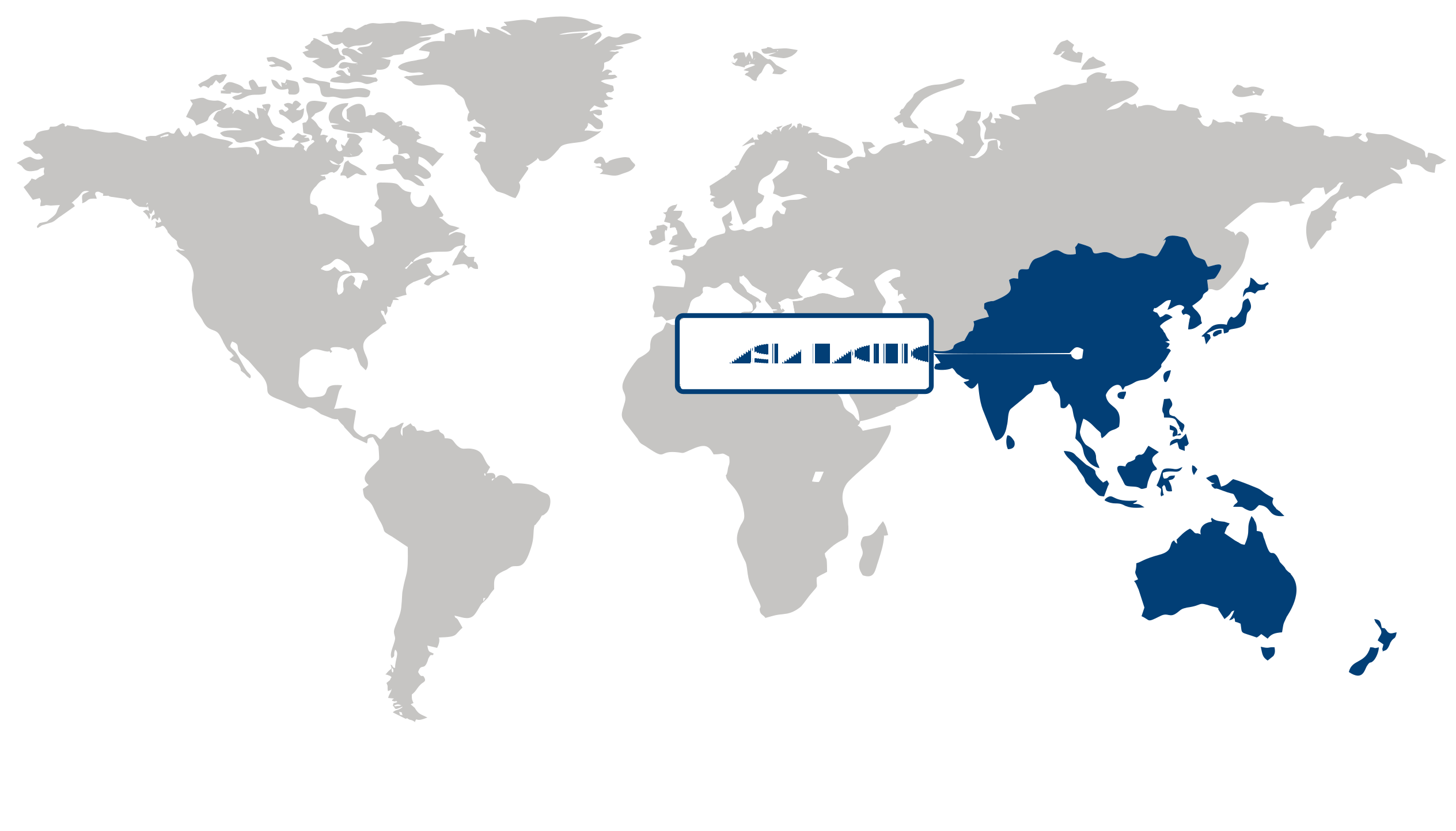
Asia Pacific (Largest & Fastest-Growing Region)
Asia Pacific accounted for the largest share of the semiconductor bonding equipment market, reaching 56.65% in 2026, and is also the fastest-growing region. The region's strong position is supported by its concentration of semiconductor manufacturing activity, expanding investments in advanced packaging, and increasing demand for sophisticated chip assembly technologies. The development of high-performance computing, artificial intelligence, consumer electronics, and automotive semiconductor applications is encouraging manufacturers to enhance production capabilities. Continued semiconductor fabrication capacity expansion and the shift toward smaller, more complex device architectures are further increasing the need for precise and efficient bonding equipment.
| Parameter | North America | Asia Pacific | Europe | Latin America | MEA |
|---|---|---|---|---|---|
| Innovation Hub i Scale Nascent Developing Advanced | |||||
| Cost-Sensitive Region i Scale Low Medium High | |||||
| Regulatory Environment i Scale Restrictive Neutral Supportive | |||||
| Demand Drivers i Scale Weak Moderate Strong | |||||
| Development Stage i Scale Emerging Developing Developed | |||||
| Adoption Rate i Scale Low Medium High | |||||
| New Entrants / Startups i Scale Sparse Moderate Dense | |||||
| Macro Indicators i Scale Weak Stable Strong |
Key Country Insights
United States 🇺🇸
Advanced Packaging InvestmentThe U.S. semiconductor industry is investing in semiconductor bonding equipment to support advanced packaging, heterogeneous integration, and high-performance chip manufacturing. Equipment suppliers are focusing on precision, automation, and higher production yields for next-generation semiconductor devices.
Germany 🇩🇪
Precision Manufacturing CapabilityGermany emphasizes semiconductor bonding equipment capable of supporting high-precision assembly for automotive, industrial, and power semiconductor applications. Manufacturers prioritize equipment delivering process stability, accuracy, and compatibility with advanced packaging technologies.
Japan 🇯🇵
High-Accuracy Bonding SystemsJapan continues to demand semiconductor bonding equipment with exceptional precision and reliability for advanced semiconductor production. Equipment investments are directed toward technologies supporting miniaturization, improved yields, and efficient manufacturing of complex electronic components.
South Korea 🇰🇷
High-Volume Packaging FocusSouth Korea is strengthening investment in semiconductor bonding equipment to support high-volume memory and logic device manufacturing. Producers increasingly seek automated systems capable of maintaining precision while improving throughput for advanced packaging processes.
France 🇫🇷
Specialized Semiconductor AssemblyFrance is adopting semiconductor bonding equipment for specialized semiconductor manufacturing serving industrial, aerospace, and research-driven applications. Buyers prioritize flexible platforms capable of supporting diverse packaging requirements and consistent process quality.
Italy 🇮🇹
Electronics Manufacturing SupportItaly is expanding the use of semiconductor bonding equipment within electronics manufacturing and specialized semiconductor assembly activities. Manufacturers increasingly value adaptable equipment that delivers reliable bonding performance while supporting evolving production requirements.
Segment Leadership and Growth Trends
Semiconductor Bonding Equipment Market Share (%), by Equipment Type, 2026
Go beyond the chart, access full insights & data tables
Request Free Sample ReportEquipment Type Segment Analysis: Wire Bonding Equipment (Largest Segment) vs Wafer Bonding Equipment (Fastest-Growing Segment)
Holding 42.12% of the market share in 2026, the wire bonding equipment segment remained the largest in the semiconductor bonding equipment market. Wire bonding continues to be extensively used because of its proven manufacturing reliability, cost efficiency, and compatibility with a broad range of semiconductor packaging applications. Its established role in high-volume integrated circuit production and mature manufacturing processes supports sustained demand from electronics manufacturers worldwide.
Wafer bonding equipment is projected to register the fastest growth as semiconductor manufacturers increasingly adopt advanced packaging technologies and three-dimensional device architectures. The growing complexity of semiconductor designs, combined with demand for higher performance, improved miniaturization, and greater functional integration, is encouraging wider implementation of wafer-level bonding processes across next-generation electronic devices.
Bonding Type Segment Analysis: Permanent Bonding (Largest Segment) vs Hybrid Bonding (Fastest-Growing Segment)
The permanent bonding segment represented the largest share of the semiconductor bonding equipment market in 2026. Permanent bonding remains essential for manufacturing semiconductor devices requiring durable mechanical strength, stable electrical performance, and long-term structural integrity. Its broad applicability across conventional semiconductor fabrication processes continues to support widespread industry adoption.
The hybrid bonding segment is anticipated to experience the fastest growth due to increasing demand for advanced semiconductor packaging capable of delivering higher interconnect density and improved electrical performance. As chip manufacturers pursue greater integration, lower power consumption, and enhanced processing capabilities, hybrid bonding is becoming an increasingly important technology for supporting future semiconductor innovations.
End Use Industry Segment Analysis: Consumer Electronics (Largest Segment) vs Automotive (Fastest-Growing Segment)
The consumer electronics industry dominated the semiconductor bonding equipment market in 2026, accounting for the largest end-use segment. Continuous production of smartphones, wearable devices, tablets, computers, and other connected electronics sustains strong demand for semiconductor bonding equipment capable of supporting high-volume manufacturing with precise assembly standards. Ongoing product innovation and device miniaturization further reinforce the segment's leadership.
The automotive industry is expected to emerge as the fastest-growing end-use segment as vehicles incorporate increasing levels of electronic content, advanced driver assistance systems, electric powertrains, and connected technologies. Growing semiconductor requirements for safety, power management, and intelligent mobility solutions are encouraging investments in advanced bonding equipment capable of supporting highly reliable automotive semiconductor manufacturing.
| Segment | Sub-Segment | Largest Segment | Fastest Growing |
|---|---|---|---|
| Equipment Type | Wire Bonding Equipment, Die Bonding Equipment, Flip Chip Bonding Equipment, Wafer Bonding Equipment | Wire Bonding Equipment | Wafer Bonding Equipment |
| Bonding Type | Permanent Bonding, Temporary Bonding, Hybrid Bonding | Permanent Bonding | Hybrid Bonding |
| End Use Industry | Consumer Electronics, Automotive, Telecommunications, Healthcare, Aerospace & Defense, Industrial, Others | Consumer Electronics | Automotive |
| Application | Advanced Packaging, Power IC and Power Discrete, Photonic Devices, MEMS Sensors and Actuators, Engineered Substrates, CMOS Image Sensors, RF Devices, Others | Advanced Packaging | Photonic Devices |
Competitive Landscape and Market Positioning
Prominent players in the semiconductor bonding equipment market:
- Applied Materials, Inc. (United States)
- Tokyo Electron Limited (Japan)
- ASMPT Limited (Hong Kong)
- Kulicke and Soffa Industries, Inc. (United States)
- BE Semiconductor Industries N.V. (Netherlands)
- EV Group (EVG) (Austria)
- SUSS MicroTec SE (Germany)
- Nidec Corporation (Japan)
- Canon, Inc. (Japan)
- Panasonic Connect Co., Ltd. (Japan)
Technological advancement is redefining rivalry in the Semiconductor Bonding Equipment Market as manufacturers compete to support increasingly sophisticated chip architectures with higher levels of accuracy and production efficiency. Equipment suppliers are investing in process innovations that improve bonding precision, accommodate advanced packaging techniques, and maintain consistent performance under demanding manufacturing conditions. The market is also placing greater emphasis on flexible equipment platforms capable of adapting to evolving semiconductor designs without extensive production reconfiguration. As fabrication requirements become more specialized, competitive strength is increasingly linked to process engineering expertise, application support, and the ability to accelerate customer qualification cycles.
| Company | Market Share | Company Revenue | Revenue CAGR (%) | Product Portfolio | Geographic Presence | Innovation / R&D Focus | Strategic Developments |
|---|---|---|---|---|---|---|---|
| Applied Materials Inc. (United States) | |||||||
| Tokyo Electron Limited (Japan) | |||||||
| ASMPT Limited (Hong Kong) | |||||||
| Kulicke and Soffa Industries Inc. (United States) | |||||||
| BE Semiconductor Industries N.V. (Netherlands) | |||||||
| EV Group (EVG) (Austria) | |||||||
| SUSS MicroTec SE (Germany) | |||||||
| Nidec Corporation (Japan) | |||||||
| Canon Inc. (Japan) | |||||||
| Panasonic Connect Co. Ltd. (Japan) |
Industry Development/News
| Company Name | Date | Key Development |
|---|---|---|
| Kulicke & Soffa | Mar-25 | Kulicke & Soffa launched ATPremier MEM PLUS, an advanced wafer-level packaging solution utilizing vertical wire technology for DRAM and NAND assembly. This commercialization targets high-volume manufacturing at the edge, addressing the stringent packaging requirements of emerging artificial intelligence applications while enhancing advanced memory density and operational efficiency. |
| Applied Materials | Jan-25 | Applied Materials acquired a 9% stake in BE Semiconductor Industries for USD 100 million to collaboratively develop hybrid bonding solutions. This strategic investment enhances the companies' joint development capabilities, accelerating the commercialization of advanced semiconductor packaging technologies necessary for high-density logic and memory applications. |
| ASMPT | Jan-25 | ASMPT commercialized the MEGA series high-precision multi-chip bonder, engineered to deliver ±2 µm bonding accuracy and throughput up to 12,000 UPH. The technology launch expands ASMPT’s portfolio for optoelectronic, RF, and AI server cluster packaging, offering manufacturers enhanced precision and capacity for complex advanced packaging operations. |
| Tokyo Electron | Dec-24 | Tokyo Electron announced a five-year, JPY 1.5 trillion research and development initiative focused on advancing packaging tools. This significant strategic investment aims to accelerate technological innovation in semiconductor bonding and integration equipment, positioning the company to address evolving manufacturing complexities in next-generation high-density chip packaging. |
| EV Group | Oct-24 | EV Group introduced the GEMINI platform, an automated production system featuring sub-micrometer alignment capabilities for 2.5D and 3D packaging architectures. This product launch enhances the company's semiconductor bonding equipment offerings, providing manufacturers with critical precision tools necessary to scale complex multi-die integration and advanced packaging operations. |
| EV Group | Aug-24 | EV Group expanded its nanoimprint lithography and wafer bonding solutions portfolio to enhance manufacturing capabilities for 3D integration. This strategic portfolio advancement strengthens support for advanced packaging applications within logic and memory device production, enabling semiconductor manufacturers to scale next-generation high-density integrated architectures. |
| TANAKA Kikinzoku Kogyo K.K. | Mar-24 | TANAKA Kikinzoku Kogyo K.K. developed an advanced gold particle bonding technology utilizing AuRoFUSE, a low-temperature fired paste. This technological innovation facilitates high-density gold-to-gold bonding, providing semiconductor manufacturers with improved mounting solutions for complex integration requirements and strengthening the commercial viability of next-generation advanced packaging architectures. |
| Tokyo Electron Kyushu | Dec-23 | Tokyo Electron Kyushu developed Extreme Laser Lift Off (XLO) technology to enhance 3D integration for advanced semiconductor devices relying on permanent wafer bonding. The technology improves precise process control and integration efficiency, equipping manufacturers with robust operational capabilities to scale high-performance semiconductor device production reliably. |
Customize Your Report
Explore examples of how this report can be tailored to different research needs, including custom segments, additional topics or chapters, and related reports. Click a section of the wheel or its numbered marker to explore the available options.
Semiconductor Bonding Equipment Market — Custom Segments
| Segment | Sub-Segment |
|---|---|
| Wafer Size | Up to 200 mm, 300 mm, 450 mm |
| Customer Type | Integrated Device Manufacturers (IDMs), Foundries, Outsourced Semiconductor Assembly and Test (OSAT) Providers, Memory Manufacturers |
| Automation Level | Manual, Semi-Automated, Fully Automated |
Semiconductor Bonding Equipment Market — Custom TOC
| Custom Chapter | Custom Details |
|---|---|
| Advanced Packaging Adoption Roadmap |
|
| Bonding Process Migration Strategies |
|
| Customer Qualification & Vendor Selection |
|
Need a different cut of the data?
Request Custom ResearchWhat is the current revenue of the semiconductor bonding equipment market?
How much is the semiconductor bonding equipment industry expected to grow by 2036?
How is semiconductor manufacturing expansion shaping demand for bonding equipment?
Why are advanced packaging technologies increasing investment in semiconductor bonding equipment?
Which equipment type leads the semiconductor bonding equipment market?
Why is the automotive industry the fastest-growing end-use segment?
Why does Asia Pacific lead the semiconductor bonding equipment market?
What is driving the fastest growth of semiconductor bonding equipment in Asia Pacific?
Which companies are driving growth in the semiconductor bonding equipment landscape?
Our Clients
"Working with FBI has been a good experience. The market report provided a holistic view, covering everything from emerging trends to potential risks."
Semtech Corporation
"The experience was highly positive. The team showcased remarkable flexibility in adapting to our specific needs and delivered report that perfectly aligned with all our requirements."
TSMC
"What really stood out to me was how clearly and promptly the Fundamental Business Insights team communicated throughout. It made the collaboration feel effortless."
NXP Semiconductors
Our Research Team & Methodology
Every Fundamental Business Insights report is built by a dedicated vertical research team, validated through a structured primary-and-secondary methodology, and reviewed for accuracy before it reaches you.
Research Team Overview
Prepared by the Electronics & Semiconductors Research Team
Delivery
Published
Demand
Available
Support
Trust & Compliance
Research Domains
10 coverage areasResearch Intelligence
| Source | Reference |
|---|---|
| Semiconductor Industry Association (SIA) | www.semiconductors.org |
| SEMI | www.semi.org |
| JEDEC Solid State Technology Association | www.jedec.org |
| IEEE | www.ieee.org |
| IPC – Association Connecting Electronics Industries | www.ipc.org |
| International Electrotechnical Commission (IEC) | www.iec.ch |
| International Organization for Standardization (ISO) | www.iso.org |
| U.S. Bureau of Industry and Security (BIS) | www.bis.gov |
| U.S. Patent and Trademark Office (USPTO) | www.uspto.gov |
| European Patent Office (EPO) | www.epo.org |
| Taiwan Semiconductor Industry Association (TSIA) | www.tsia.org.tw |
| World Semiconductor Trade Statistics (WSTS) | www.wsts.org |
| International Energy Agency (IEA) | www.iea.org |
| GSMA | www.gsma.com |
| 3GPP | www.3gpp.org |
| ITU (International Telecommunication Union) | www.itu.int |
| Omdia (public insights) | omdia.tech.informa.com |
| Display Supply Chain Consultants (DSCC) | www.displaysupplychain.com |
| U.S. Department of Energy (DOE) | www.energy.gov |
| NIST (National Institute of Standards and Technology) | www.nist.gov |
Research Workflow & Quality Assurance
Data Collection
Verified information gathered through primary and secondary research.
Data Triangulation
Cross-validation using multiple independent data sources.
Forecast Modelling
Market estimates developed using historical trends and analytical models.
Analyst Validation
Findings reviewed by domain experts for accuracy and consistency.
Editorial & Quality Review
Final editorial, quality, and compliance checks before publication.
Final Publication
Released after successful completion of the internal review process.
Report Coverage
📊 Market Assessment
- Market Size & Forecast
- Market Segmentation
- Regional Analysis
- Growth Drivers & Challenges
- Market Dynamics
🏢 Competitive Intelligence
- Competitive Landscape
- Company Profiles
- Competitive Benchmarking
- Mergers & Acquisitions
- Market Share Analysis or Key Company Strategies
🔍 Strategic Analysis
- Value Chain Analysis
- Porter's Five Forces
- PESTLE Analysis
- Pricing Trends
- Supply-Demand Analysis
🚀 Future Outlook
- Technology Landscape
- Regulatory Landscape
- Investment & Funding Landscape
- Emerging Opportunities
- Future Market Outlook
Have a question about this report or need a custom scope?
Request Customization